ꢀ ꢁꢂꢃ ꢄ ꢅ ꢆꢇ ꢈꢉ ꢀ ꢊꢋ ꢀ ꢁꢂꢃ ꢌ ꢍ ꢎꢏꢐ ꢀꢋ ꢀ ꢁꢂꢃ ꢄꢑ ꢒ ꢏꢐ ꢎ
ꢕ
ꢉ
ꢊ
ꢈ
ꢊ
ꢓ
ꢐ
ꢀꢔ
ꢁ
ꢏ
ꢓ
ꢁꢕ
ꢆ
ꢊ
ꢋ
ꢀ
ꢕ
ꢖ
ꢔ
ꢂ
ꢕ
ꢀ
ꢗ
ꢐ
ꢉ
ꢊ
ꢋ
ꢀ
ꢖꢔ
ꢁ
ꢕ
ꢖ
ꢊ
ꢓ
ꢋ
ꢕ ꢁꢊꢓ ꢐꢗ ꢇꢕ ꢈꢐꢀ ꢐꢘꢁ ꢀꢇ ꢙ ꢇꢊ ꢓꢆ
ꢓ
ꢐ
ꢇ
ꢀ
ꢔ
ꢗ
ꢕ
ꢔ
ꢓ
ꢐ
ꢇ
ꢀ
ꢕ
ꢏ
ꢗ
ꢁ
ꢏ
ꢗ
SLOS433I − FEBRUARY 2004 − REVISED MARCH 2005
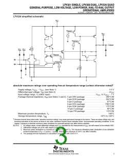
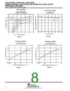
LPV324 simplified schematic
V
CC
V
BIAS1
V
CC
+
−
V
BIAS2
+
Output
−
V
V
CC CC
V
BIAS3
+
IN−
IN+
−
V
BIAS4
+
−
†
absolute maximum ratings over operating free-air temperature range (unless otherwise noted)
Supply voltage, V
− V
(see Note 1) . . . . . . . . . . . . . . . . . . . . . . . . . . . . . . . . . . . . . . . . . . . . . . . . . . . 5.5 V
CC+
CC−
ID
Differential input voltage, V (see Note 2) . . . . . . . . . . . . . . . . . . . . . . . . . . . . . . . . . . . . . . . . . . . . . . . . . . .
Input voltage range, V (either input) . . . . . . . . . . . . . . . . . . . . . . . . . . . . . . . . . . . . . . . . . . . . V
V
CC
− 1 V
to V
I
CC−
CC+
Package thermal impedance, θ (see Notes 3 and 4): 5-pin DBV package . . . . . . . . . . . . . . . . . . . 206°C/W
JA
5-pin DCK package . . . . . . . . . . . . . . . . . . . 252°C/W
8-pin D package . . . . . . . . . . . . . . . . . . . . . . . 97°C/W
8-pin DDU package . . . . . . . . . . . . . . . . . . TBD°C/W
8-pin DGK package . . . . . . . . . . . . . . . . . . . 172°C/W
14-pin D package . . . . . . . . . . . . . . . . . . . . . . 86°C/W
14-pin PW package . . . . . . . . . . . . . . . . . . . 113°C/W
Maximum junction temperature, T . . . . . . . . . . . . . . . . . . . . . . . . . . . . . . . . . . . . . . . . . . . . . . . . . . . . . . . . . 150°C
J
Storage temperature range, T
. . . . . . . . . . . . . . . . . . . . . . . . . . . . . . . . . . . . . . . . . . . . . . . . . . . −65°C to 150°C
stg
†
Stresses beyond those listed under “absolute maximum ratings” may cause permanent damage to the device. These are stress ratings only, and
functional operation of the device at these or any other conditions beyond those indicated under “recommended operating conditions” is not
implied. Exposure to absolute-maximum-rated conditions for extended periods may affect device reliability.
NOTES: 1. All voltage values, except differential voltages and V
2. Differential voltages are at IN+ with respect to IN−.
specified for the measurement of I , are with respect to the network GND.
CC
OS
3. Maximum power dissipation is a function of T (max), θ , and T . The maximum allowable power dissipation at any allowable
JA
J
A
ambient temperature is P = (T (max) − T )/θ . Selecting the maximum of 150°C can affect reliability.
D
J
A
JA
4. The package thermal impedance is calculated in accordance with JESD 51-7.
3
POST OFFICE BOX 655303 • DALLAS, TEXAS 75265

 TI [ TEXAS INSTRUMENTS ]