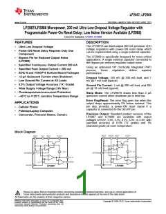
LP2987, LP2988
SNVS004J –MARCH 1999–REVISED APRIL 2013
www.ti.com
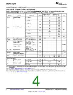
ELECTRICAL CHARACTERISTICS (continued)
Limits in standard typeface are for TJ = 25°C, and limits in boldface type apply over the full operating temperature range.
Unless otherwise specified: VIN = VO(NOM) + 1V, IL = 1 mA, COUT = 4.7 µF, CIN = 2.2 µF, VS/D = 2V.
(1)
(1)
LM2987/8AI-X.X
LM2987/8I-X.X
Symbol
VIN–VO
Parameter
Conditions
IL = 100 µA
Typical
1
Units
Min
Max
2.0
Min
Max
2.0
Dropout Voltage
(2)
3.5
3.5
120
170
230
350
120
150
800
1400
2.1
IL = 75 mA
IL = 200 mA
IL = 100 µA
IL = 75 mA
IL = 200 mA
VS/D < 0.3V
120
170
230
350
120
150
800
90
mV
180
100
500
1
IGND
Ground Pin Current
µA
1400
2.1
mA
µA
3.7
3.7
0.05
400
400
1.5
1.5
IO(PK)
IO(MAX)
en
Peak Output Current
Short Circuit Current
VOUT ≥ VO(NOM) − 5%
250
250
mA
(3)
RL = 0 (Steady State)
LP2987 Output Noise
Voltage (RMS)
BW = 300 Hz to
50 kHz, VOUT = 3.3V
COUT = 10 µF
100
µV(RMS)
LP2988 Output Noise
Voltage (RMS)
BW = 300 Hz to 50 kHz,
VOUT = 3.3V
COUT = 10 µF
20
CBYPASS = .01 µF
ΔVOUT/ΔVIN
ΔVOUT/ΔT
IDELAY
Ripple Rejection
f = 1 kHz, COUT = 10 µF
CBYP = 0 (LP2988)
(4)
65
20
dB
Output Voltage
Temperature Coefficient
ppm/°C
Delay Pin Current Source
1.6
2.8
1.6
2.8
2.2
µA
1.4
3.0
1.4
3.0
SHUTDOWN INPUT
VS/D
S/D Input Voltage
VH = O/P ON
VL = O/P OFF
VS/D = 0
1.4
0.55
0
1.6
1.6
(5)
V
0.18
−1
0.18
−1
IS/D
S/D Input Current
µA
VS/D = 5V
5
15
15
(2) Dropout voltage is defined as the input to output differential at which the output voltage drops 100 mV below the value measured with a
1V differential.
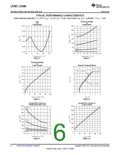
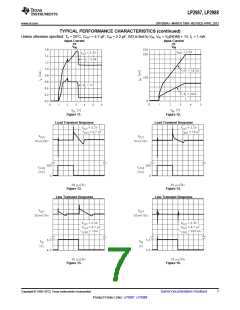
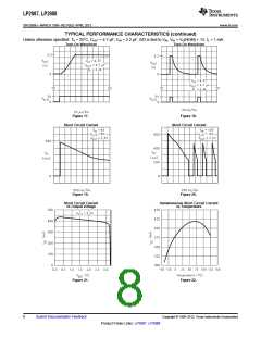
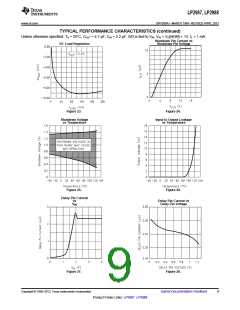
(3) See TYPICAL PERFORMANCE CHARACTERISTICS curves.
(4) Temperature coefficient is defined as the maximum (worst-case) change divided by the total temperature range.
(5) To prevent mis-operation, the Shutdown input must be driven by a signal that swings above VH and below VL with a slew rate not less
than 40 mV/µs (see APPLICATION HINTS).
4
Submit Documentation Feedback
Copyright © 1999–2013, Texas Instruments Incorporated
Product Folder Links: LP2987 LP2988

 TI [ TEXAS INSTRUMENTS ]