LMV321 SINGLE, LMV358 DUAL, LMV324 QUAD
LOW-VOLTAGE RAIL-TO-RAIL OUTPUT OPERATIONAL AMPLIFIERS
SLOS263C – AUGUST 1999 – REVISED MARCH 2000
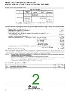
AVAILABLE OPTIONS
PACKAGED DEVICES
PACKAGE
TYPE
T
A
SINGLE
DUAL
QUADRUPLE
LMV321IDCKR
LMV321IDBVR
—
—
—
—
5-pin SOT
8-pin SOIC
8-pin TSSOP
—
—
LMV358ID
LMV358IPWR
—
—
–40°C to 85°C
14-pin SOIC
14-pin TSSOP
—
—
LMV324ID
LMV324IPWR
—
The D package is available taped and reeled. Add the suffix R to the device type (e.g.,
LMV324DR).TheDCK, DBV, andPWpackagesareonlyavailableleft-endtapedandreeled.
†
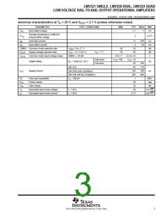
absolute maximum ratings over operating free-air temperature range (unless otherwise noted)
Supply voltage, V
(see Note 1) . . . . . . . . . . . . . . . . . . . . . . . . . . . . . . . . . . . . . . . . . . . . . . . . . . . . . . . . . . . 5.5 V
CC
Differential input voltage, V (see Note 2) . . . . . . . . . . . . . . . . . . . . . . . . . . . . . . . . . . . . . . . . . . . . . . . . . . ±5.5 V
ID
Input voltage, V (either input) . . . . . . . . . . . . . . . . . . . . . . . . . . . . . . . . . . . . . . . . . . . . . . . . . . . . . . . . . . 0 to 5.5 V
I
Duration of output short circuit (one amplifier) to ground at (or below) T = 25°C,
A
V
≤ 5.5 V (see Note 3) . . . . . . . . . . . . . . . . . . . . . . . . . . . . . . . . . . . . . . . . . . . . . . . . . . . . . . . . . . . . . Unlimited
CC
Operating virtual junction temperature . . . . . . . . . . . . . . . . . . . . . . . . . . . . . . . . . . . . . . . . . . . . . . . . . . . . . . 150°C
Package thermal impedance, θ (see Notes 4 and 5): D (8-pin) package . . . . . . . . . . . . . . . . . . . . . 197°C/W
JA
D (14-pin) package . . . . . . . . . . . . . . . . . . . 127°C/W
DBV package . . . . . . . . . . . . . . . . . . . . . . . . 347°C/W
DCK package . . . . . . . . . . . . . . . . . . . . . . . . 389°C/W
PW (8-pin) package . . . . . . . . . . . . . . . . . . . 243°C/W
PW (14-pin) package . . . . . . . . . . . . . . . . . . 170°C/W
Lead temperature 1,6 mm (1/16 inch) from case for 10 seconds: D or PW package . . . . . . . . . . . . . . 260°C
DBV or DCK package . . . . . . . . . . . . . TBD
Storage temperature range, T
. . . . . . . . . . . . . . . . . . . . . . . . . . . . . . . . . . . . . . . . . . . . . . . . . . . . . –65 to 150°C
stg
†
Stresses beyond those listed under “absolute maximum ratings” may cause permanent damage to the device. These are stress ratings only, and
functional operation of the device at these or any other conditions beyond those indicated under “recommended operating conditions” is not
implied. Exposure to absolute-maximum-rated conditions for extended periods may affect device reliability.
NOTES: 1. All voltage values (except differential voltages and V
2. Differential voltages are at IN+ with respect to IN–.
specified for the measurement of I ) are with respect to the network GND.
OS
CC
3. Short circuits from outputs to V
4. Maximum power dissipation is a function of T (max), θ , and T . The maximum allowable power dissipation at any allowable
can cause excessive heating and eventual destruction.
CC
J
JA
A
ambient temperature is P = (T (max) – T )/θ . Selecting the maximum of 150°C can impact reliability.
D
J
A
JA
5. The package thermal impedance is calculated in accordance with JESD 51.
recommended operating conditions
MIN
2.7
MAX
5.5
UNIT
V
V
Supply voltage (single-supply operation)
Operating free-air temperature
CC
T
A
–40
85
°C
2
POST OFFICE BOX 655303 • DALLAS, TEXAS 75265

 TI [ TEXAS INSTRUMENTS ]