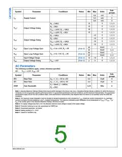
Sub-
groups
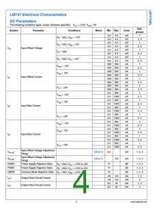
Symbol
Parameter
Conditions
Notes
Min Max
Units
5.6
mA
mA
mA
V
1
ICC
Supply Current
5.0
2
3
6.6
12
1, 2, 3
RL = 10KΩ
RL = 2KΩ
10
V
V
V
V
V
V
V
1, 2, 3
1, 2, 3
1, 2, 3
1, 2, 3
1, 2, 3
1, 2, 3
1, 2, 3
+
VOP
Output Voltage Swing
Output Voltage Swing
16
VCC = ±20V, RL = 10KΩ
VCC = ±20V, RL = 2KΩ
RL = 10KΩ
15
-12
-10
-16
-15
RL = 2KΩ
-
VOP
VCC = ±20V, RL = 10KΩ
VCC = ±20V, RL = 2KΩ
50
25
50
25
V/mV
V/mV
V/mV
V/mV
V
1
+
-
AVS
VO = 0 to +10V, RL = 2K
VO = 0 to -10V, RL = 2K
Open Loop Voltage Gain
Open Loop Voltage Gain
(Note 6)
(Note 6)
2, 3
1
AVS
2, 3
VI
Input Voltage Range
Output Voltage Swing
(Note 4)
(Note 5)
12
2
−12
−2
1, 2, 3
1, 2, 3
VOP
VCC = ±5V
V
AC Parameters
The following conditions apply, unless otherwise specified.
AC:
VCC = ±15V, VCM = 0V
Sub-
groups
Symbol
Parameter
Conditions
Notes
Min Max
Units
SR+
Slew Rate
Slew Rate
AV = 1, VI = -5V to +5V
AV = 1, VI = +5V to -5V
VI = 50mV, ƒ = 20KHz,
RL = 2KΩ
0.2
0.2
V/µS
V/µS
9
9
SR-
GBW
Gain Bandwidth
0.25
Mhz
9
Note 1: Absolute Maximum Ratings indicate limits beyond which damage to the device may occur. Operating Ratings indicate conditions for which the device is
functional, but do not guarantee specific performance limits. For guaranteed specifications and test conditions, see the Electrical Characteristics. The guaranteed
specifications apply only for the test conditions listed. Some performance characteristics may degrade when the device is not operated under the listed test
conditions.
Note 2: The maximum power dissipation must be derated at elevated temperatures and is dictated by TJmax (maximum junction temperature), θJA (package
junction to ambient thermal resistance), and TA (ambient temperature). The maximum allowable power dissipation at any temperature is PDmax = (TJmax - TA)/
θ
JA or the number given in the Absolute Maximum Ratings, whichever is lower.
Note 3: For supply voltages less than ±15V, the absolute maximum input voltage is equal to the supply voltage.
Note 4: Parameter tested go-no-go only, guaranteed by CMRR test.
Note 5: Guaranteed parameter, not tested.
Note 6: Datalog reading in K = V/mV
Note 7: Tested for CERDIPs only.
www.national.com
4

 TI [ TEXAS INSTRUMENTS ]