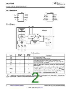
DAC081S101
SNAS323C –JUNE 2005–REVISED FEBRUARY 2013
www.ti.com
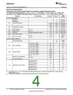
AC and Timing Characteristics
Values shown in this table are design targets and are subject to change before product release.
The following specifications apply for VA = +2.7V to +5.5V, RL = 2kΩ to GND, CL = 200 pF to GND, fSCLK = 30 MHz, input
code range 4 to 251. Boldface limits apply for TMIN ≤ TA ≤ TMAX: all other limits TA = 25°C, unless otherwise specified.
Units
(Limits)
Parameter
Test Conditions
Typical
Limits
fSCLK
ts
SCLK Frequency
30
5
MHz (max)
Output Voltage Settling Time
40h to C0h code
change, RL = 2kΩ
CL ≤ 200 pF
3
µs (max)
(1)
SR
Output Slew Rate
Glitch Impulse
1
12
0.5
6
V/µs
nV-sec
nV-sec
µs
Code change from 80h to 7Fh
Digital Feedthrough
VA = 5V
VA = 3V
tWU
Wake-Up Time
39
µs
1/fSCLK
SCLK Cycle Time
SCLK High time
SCLK Low Time
33
13
13
ns (min)
ns (min)
ns (min)
tH
tL
5
5
Set-up Time SYNC to SCLK Rising
Edge
tSUCL
−15
0
ns (min)
tSUD
tDHD
Data Set-Up Time
Data Hold Time
2.5
2.5
0
5
4.5
3
ns (min)
ns (min)
ns (min)
ns (min)
ns (min)
ns (min)
VA = 5V
tCS
SCLK fall to rise of SYNC
SYNC High Time
VA = 3V
−2
9
1
2.7 ≤ VA ≤ 3.6
3.6 ≤ VA ≤ 5.5
20
10
tSYNC
5
(1) This parameter is guaranteed by design and/or characterization and is not tested in production.
Specification Definitions
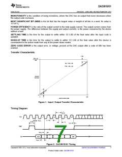
DIFFERENTIAL NON-LINEARITY (DNL) is the measure of the maximum deviation from the ideal step size of 1
LSB, which is VREF / 256 = VA / 256.
DIGITAL FEEDTHROUGH is a measure of the energy injected into the analog output of the DAC from the digital
inputs when the DAC outputs are not updated. It is measured with a full-scale code change on the data bus.
FULL-SCALE ERROR is the difference between the actual output voltage with a full scale code (FFh) loaded
into the DAC and the value of VA x 255 / 256.
GAIN ERROR is the deviation from the ideal slope of the transfer function. It can be calculated from Zero and
Full-Scale Errors as GE = FSE - ZE, where GE is Gain error, FSE is Full-Scale Error and ZE is Zero Error.
GLITCH IMPULSE is the energy injected into the analog output when the input code to the DAC register
changes. It is specified as the area of the glitch in nanovolt-seconds.
INTEGRAL NON-LINEARITY (INL) is a measure of the deviation of each individual code from a straight line
through the input to output transfer function. The deviation of any given code from this straight line is measured
from the center of that code value. The end point method is used. INL for this product is specified over a limited
range, per the Electrical Tables.
LEAST SIGNIFICANT BIT (LSB) is the bit that has the smallest value or weight of all bits in a word. This value is
LSB = VREF / 2n
(1)
where VREF is the supply voltage for this product, and "n" is the DAC resolution in bits, which is 8 for the
DAC081S101.
MAXIMUM LOAD CAPACITANCE is the maximum capacitance that can be driven by the DAC with output
stability maintained.
6
Submit Documentation Feedback
Copyright © 2005–2013, Texas Instruments Incorporated
Product Folder Links: DAC081S101

 TI [ TEXAS INSTRUMENTS ]