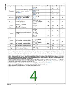
Symbol
Parameter
Conditions
CGATE = 0
Min
Typ
Max
85
Unit
-
25
(Note 6)
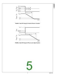
Gate Capacitance Discharge Time at
Forward to Reverse Transition
See Figure 3
CGATE = 10 nF
(Note 6)
tGATE(REV)
-
-
60
-
ns
CGATE = 47 nF
(Note 6)
180
350
Gate Capacitance DischargeTime at
OFF pin Low to High Transition
See Figure 4
CGATE = 47 nF
tGATE(OFF)
-
486
2.8
-
-
ns
A
(Note 7)
VGATE = VIN + 3V
VOUT > VIN + 100 mV
IGATE(OFF)
Gate Pin Sink Current
1.8
t ≤ 10ms
Reverse VSD Threshold
VIN < VOUT
VSD(REV)
VIN - VOUT
-41
-28
10
-16
mV
mV
Reverse VSD Hysteresis
ΔVSD(REV)
-
-
VIN = 5.0V
VVS = VIN
VIN - VOUT
1
19
22
37
37
Regulated Forward VSD Threshold
VIN > VOUT
VSD(REG)
mV
VIN = 12.0V
VVS = VIN
4.4
VIN - VOUT
OFF Pin
VOUT = VIN-500 mV
VOFF Rising
VOFF(IH)
OFF Input High Threshold Voltage
-
1.56
1.40
1.75
V
VOUT = VIN - 500 mV
VOFF Falling
VOFF(IL)
ΔVOFF
IOFF
OFF Input Low Threshold Voltage
OFF Threshold Voltage Hysteresis
OFF Pin Internal Pull-down
1.10
-
VOFF(IH) - VOFF(IL)
VOFF = 4.5V
-
3.0
-
155
5
-
7.0
-
mV
µA
VOFF = 5.0V
8
Note 1: Absolute Maximum Ratings indicate limits beyond which damage to the device may occur, including in-operability and degradation of device reliability
and/or performance. Functional operation of the device and/or non-degradation at the Absolute Maximum Ratings or other conditions beyond those indicated in
the Recommended Operating Conditions is not implied. Operating Range conditions indicate the conditions at which the device is functional and the device should
not be operated beyond such conditions. For guaranteed specifications and conditions, see the Electrical Characteristics table.
Note 2: The Human Body Model (HBM) is a 100 pF capacitor discharged through a 1.5 kΩ resistor into each pin. Applicable test standard is JESD-22-A114-C.
Note 3: The Machine Model (MM) is a 200 pF capacitor discharged through a 0Ω resistor (i.e. directly) into each pin. Applicable test standard is JESD-A115-A.
Note 4: For soldering specifications see the LM5050-1 Product Folder at www.national.com, general information at www.national.com/analog/packaging/, and
reflow information at www.national.com/ms/MS/MS-SOLDERING.pdf .
Note 5: The GATE pin voltage is typically 12V above the IN pin voltage when the LM5050-1 is enabled (i.e. OFF Pin is Open or Low, and VIN > VOUT). Therefore,
the Absolute Maximum Rating for the IN pin voltage applies only when the LM5050-1 is disabled (i.e. OFF Pin is logic high), or for a momentary surge to that
voltage since the Absolute Maximum Rating for the GATE pin is also 100V
Note 6: Time from VIN-VOUT voltage transition from 200 mV to -500 mV until GATE pin voltage falls to VIN + 1V. See Figure 3
Note 7: Time from VOFF voltage transition from 0.0V to 5.0V until GATE pin voltage falls to VIN + 1V. See Figure 4
Note 8: Measurement of VGS voltage (i.e. VGATE - VIN) includes 1 MΩ in parallel with CGATE
.
www.ti.com
4

 TI [ TEXAS INSTRUMENTS ]