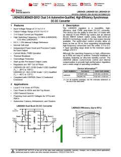
LM26420, LM26420-Q0, LM26420-Q1
www.ti.com
SNVS579J –FEBRUARY 2009–REVISED SEPTEMBER 2015
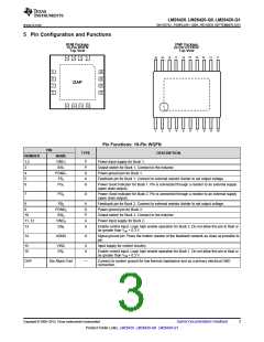
5 Pin Configuration and Functions
RUM Package
16-Pin WQFN
Top View
PWP Package
20-Pin HTSSOP
Top View
15
14 13
12
11
19
18 17
16
3
2
4
1
20
16
15
14
13
5
6
7
8
DAP
10
11
9
12
3
7
8
9
10
1
2
4
6
5
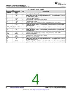
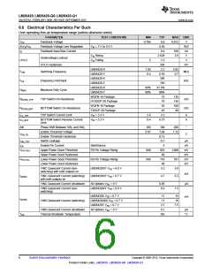
Pin Functions: 16-Pin WQFN
PIN
TYPE
DESCRIPTION
NUMBER
NAME
VIND1
SW1
1,2
3
P
P
G
A
G
Power input supply for Buck 1.
Output switch for Buck 1. Connect to the inductor.
Power ground pin for Buck 1.
4
PGND1
FB1
5
Feedback pin for Buck 1. Connect to external resistor divider to set output voltage.
6
PG1
Power Good Indicator for Buck 1. Pin is connected through a resistor to an external supply
(open drain output).
7
PG2
G
Power Good Indicator for Buck 2. Pin is connected through a resistor to an external supply
(open drain output).
8
FB2
PGND2
SW2
A
G
P
A
A
Feedback pin for Buck 2. Connect to external resistor divider to set output voltage.
Power ground pin for Buck 2.
9
10
Output switch for Buck 2. Connect to the inductor.
Power Input supply for Buck 2.
11, 12
13
VIND2
EN2
Enable control input. Logic high enable operation for Buck 2. Do not allow this pin to float or
be greater than VIN + 0.3 V.
14
AGND
G
Signal ground pin. Place the bottom resistor of the feedback network as close as possible to
pin.
15
16
VINC
EN1
A
A
Input supply for control circuitry.
Enable control input. Logic high enable operation for Buck 1. Do not allow this pin to float or
be greater than VIN + 0.3 V.
DAP
Die Attach Pad
—
Connect to system ground for low thermal impedance and as a primary electrical GND
connection.
Copyright © 2009–2015, Texas Instruments Incorporated
Submit Documentation Feedback
3
Product Folder Links: LM26420 LM26420-Q0 LM26420-Q1

 TI [ TEXAS INSTRUMENTS ]