LM2597, LM2597HV
www.ti.com
SNVS119C –MARCH 1998–REVISED APRIL 2013
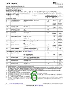
All Output Voltage Versions
Electrical Characteristics
(continued)
Specifications with standard type face are for TJ = 25°C, and those with boldface type apply over full Operating
Temperature Range. Unless otherwise specified, VIN = 12V for the 3.3V, 5V, and Adjustable version and VIN = 24V for the
12V version. ILOAD = 100 mA.
Symbol
Parameter
Conditions
LM2597/LM2597HV-XX
Units
(Limits)
(1)
(2)
Typ
Limit
FLAG/DELAY CONTROL Test Circuit of Figure 31
Regulator Dropout
Detector
Threshold Voltage
Low (Flag ON)
96
%
%(min)
%(max)
V
92
98
VFSAT
IFL
Flag Output Saturation
Voltage
ISINK = 3 mA
VDELAY = 0.5V
VFLAG = 40V
0.3
0.3
0.7/1.0
V(max)
μA
Flag Output Leakage
Current
Delay Pin Threshold
Voltage
1.25
V
Low (Flag ON)
1.21
1.29
V(min)
V(max)
μA
High (Flag OFF) and VOUT Regulated
VDELAY = 0.5V
Delay Pin Source
Current
3
6
μA(max)
mV
Delay Pin Saturation
Low (Flag ON)
55
350/400
mV(max)
BIAS SUPPLY
IBS Bias Supply Pin Current
(9)
VBS = 2V
120
4
μA
μA(max)
mA
400
(9)
VBS = 4.4V
10
2
mA(max)
mA
(9)
IQ
Operating Quiescent Current VBS = 4.4V , Vin pin current
1
(9) Feedback pin removed from output and connected to 12V for the 3.3V, 5V, and the ADJ. version, and 15V for the 12V version, to force
the output transistor switch OFF.
Copyright © 1998–2013, Texas Instruments Incorporated
Submit Documentation Feedback
7
Product Folder Links: LM2597 LM2597HV

 TI [ TEXAS INSTRUMENTS ]