LM2597, LM2597HV
www.ti.com
SNVS119C –MARCH 1998–REVISED APRIL 2013
THERMAL CONSIDERATIONS
The LM2597/LM2597HV is available in two packages, an 8-pin through hole PDIP (P) and an 8-pin surface
mount SOIC-8 (D). Both packages are molded plastic with a copper lead frame. When the package is soldered to
the PC board, the copper and the board are the heat sink for the LM2597 and the other heat producing
components.
For best thermal performance, wide copper traces should be used. Pins should be soldered to generous
amounts of printed circuit board copper, (one exception to this is the output (switch) pin, which should not have
large areas of copper). Large areas of copper provide the best transfer of heat (lower thermal resistance) to the
surrounding air, and even double-sided or multilayer boards provide a better heat path to the surrounding air.
Unless power levels are small, sockets are not recommended because of the added thermal resistance it adds
and the resultant higher junction temperatures.
Package thermal resistance and junction temperature rise numbers are all approximate, and there are many
factors that will affect the junction temperature. Some of these factors include board size, shape, thickness,
position, location, and even board temperature. Other factors are, trace width, printed circuit copper area, copper
thickness, single- or double-sided, multilayer board, and the amount of solder on the board. The effectiveness of
the PC board to dissipate heat also depends on the size, quantity and spacing of other components on the
board. Furthermore, some of these components such as the catch diode will add heat to the PC board and the
heat can vary as the input voltage changes. For the inductor, depending on the physical size, type of core
material and the DC resistance, it could either act as a heat sink taking heat away from the board, or it could add
heat to the board.
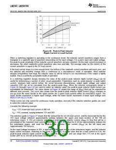
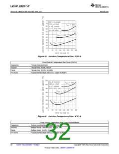
The curves shown in Figure 41 and Figure 42 show the LM2597 junction temperature rise above ambient
temperature with a 500 mA load for various input and output voltages. The Bias Supply pin was not used (left
open) for these curves. Connecting the Bias Supply pin to the output voltage would reduce the junction
temperature by approximately 5°C to 15°C, depending on the input and output voltages, and the load current.
This data was taken with the circuit operating as a buck switcher with all components mounted on a PC board to
simulate the junction temperature under actual operating conditions. This curve is typical, and can be used for a
quick check on the maximum junction temperature for various conditions, but keep in mind that there are many
factors that can affect the junction temperature.
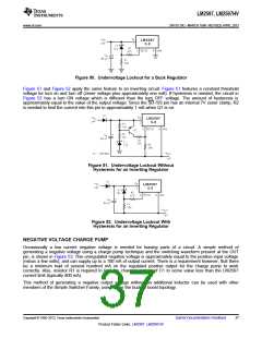
BIAS SUPPLY FEATURE
The bias supply (VBS) pin allows the LM2597's internal circuitry to be powered from a power source, other than
VIN, typically the output voltage. This feature can increase efficiency and lower junction temperatures under some
operating conditions. The greatest increase in efficiency occur with light load currents, high input voltage and low
output voltage (4V to 12V). See efficiency curves shown in Figure 43 and Figure 44. The curves with solid lines
are with the VBS pin connected to the regulated output voltage, while the curves with dashed lines are with the
VBS pin open.
The bias supply pin requires a minimum of approximately 3.5V at room temperature (4V @ −40°C), and can be
as high as 30V, but there is little advantage of using the bias supply feature with voltages greater than 15V or
20V. The current required for the VIN pin is typically 4 mA.
To use the bias supply feature with output voltages between 4V and 15V, wire the bias pin to the regulated
output. Since the VBS pin requires a minimum of 4V to operate, the 3.3V part cannot be used this way. When the
VBS pin is left open, the intemal regulator circuitry is powered from the input voltage.
Copyright © 1998–2013, Texas Instruments Incorporated
Submit Documentation Feedback
33
Product Folder Links: LM2597 LM2597HV

 TI [ TEXAS INSTRUMENTS ]