LM2597, LM2597HV
SNVS119C –MARCH 1998–REVISED APRIL 2013
www.ti.com
APPLICATION INFORMATION
PIN FUNCTIONS
+VIN (Pin 7)This is the positive input supply for the IC switching regulator. A suitable input bypass capacitor must
be present at this pin to minimize voltage transients and to supply the switching currents needed by the
regulator.
Ground (Pin 6)Circuit ground
Output (Pin 8)Internal switch
The voltage at this pin switches between (+VIN − VSAT) and approximately −0.5V, with a duty
cycle of VOUT/VIN. To minimize coupling to sensitive circuitry, the PC board copper area
connected to this pin should be kept to a minimum.
Feedback (Pin 4)Senses the regulated output voltage to complete the feedback loop.
Shutdown /Soft-start (Pin 5)This dual function pin provides the following features: (a) Allows the switching
regulator circuit to be shut down using logic level signals thus dropping the total input supply current to
approximately 80 μA. (b) Adding a capacitor to this pin provides a soft-start feature which minimizes
startup current and provides a controlled ramp up of the output voltage.
Error Flag (Pin 1)Open collector output that provides a low signal (flag transistor ON) when the regulated output
voltage drops more than 5% from the nominal output voltage. On start up, Error Flag is low until VOUT
reaches 95% of the nominal output voltage and a delay time determined by the Delay pin capacitor. This
signal can be used as a reset to a microprocessor on power-up.
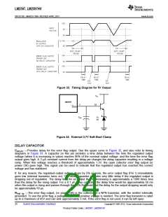
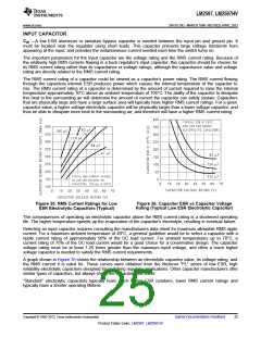
Delay (Pin 2)At power-up, this pin can be used to provide a time delay between the time the regulated output
voltage reaches 95% of the nominal output voltage, and the time the error flag output goes high.
Bias Supply (Pin 3)This feature allows the regulators internal circuitry to be powered from the regulated output
voltage or an external supply, instead of the input voltage. This results in increased efficiency under some
operating conditions, such as low output current and/or high input voltage.
NOTE
If any of the above four features (Shutdown /Soft-start, Error Flag, Delay, or Bias Supply)
are not used, the respective pins should be left open.
EXTERNAL COMPONENTS
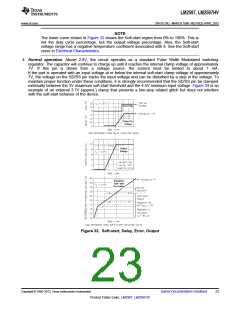
SOFT-START CAPACITOR
CSS —A capacitor on this pin provides the regulator with a Soft-start feature (slow start-up). When the DC input
voltage is first applied to the regulator, or when the Shutdown /Soft-start pin is allowed to go high, a constant
current (approximately 5 μA begins charging this capacitor). As the capacitor voltage rises, the regulator goes
through four operating regions (See the bottom curve in Figure 32).
1. Regulator in Shutdown. When the SD /SS pin voltage is between 0V and 1.3V, the regulator is in
shutdown, the output voltage is zero, and the IC quiescent current is approximately 85 μA.
2. Regulator ON, but the output voltage is zero. With the SD /SS pin voltage between approximately 1.3V
and 1.8V, the internal regulatory circuitry is operating, the quiescent current rises to approximately 5 mA, but
the output voltage is still zero. Also, as the 1.3V threshold is exceeded, the Soft-start capacitor charging
current decreases from 5 μA down to approximately 1.6 μA. This decreases the slope of capacitor voltage
ramp.
3. Soft-start Region. When the SD /SS pin voltage is between 1.8V and 2.8V (@ 25°C), the regulator is in a
Soft-start condition. The switch (Pin 8) duty cycle initially starts out very low, with narrow pulses and
gradually get wider as the capacitor SD /SS pin ramps up towards 2.8V. As the duty cycle increases, the
output voltage also increases at a controlled ramp up. See the center curve in Figure 32. The input supply
current requirement also starts out at a low level for the narrow pulses and ramp up in a controlled manner.
This is a very useful feature in some switcher topologies that require large startup currents (such as the
inverting configuration) which can load down the input power supply.
22
Submit Documentation Feedback
Copyright © 1998–2013, Texas Instruments Incorporated
Product Folder Links: LM2597 LM2597HV

 TI [ TEXAS INSTRUMENTS ]