LM1881
SNLS384F –FEBRUARY 1995–REVISED MARCH 2013
www.ti.com
(1)(2)
Absolute Maximum Ratings
Supply Voltage
13.2V
Input Voltage
3 VP-P (VCC = 5V)
6 VP-P (VCC ≥ 8V)
Output Sink Currents; Pins, 1, 3, 5
Output Sink Current; Pin 7
5 mA
2 mA
(3)
Package Dissipation
1100 mW
−65°C to +150°C
2 kV
Storage Temperature Range
(4)
ESD Susceptibility
(5)
ESD Susceptibility
200 V
Soldering Information
PDIP Package (10 sec.)
SOIC Package
260°C
Vapor Phase (60 sec.)
Infrared (15 sec.)
215°C
220°C
(1) Absolute Maximum Ratings indicate limits beyond which damage to the device may occur. For ensured specifications and test
conditions, see the Electrical Characteristics. The ensured specifications apply only for the test conditions listed.
(2) If Military/Aerospace specified devices are required, please contact the TI Sales Office/ Distributors for availability and specifications.
(3) For operation in ambient temperatures above 25°C, the device must be derated based on a 150°C maximum junction temperature and a
package thermal resistance of 110°C/W, junction to ambient.
(4) ESD susceptibility test uses the “human body model, 100 pF discharged through a 1.5 kΩ resistor”.
(5) Machine Model, 220 pF – 240 pF discharged through all pins.
Electrical Characteristics LM1881
VCC = 5V; RSET = 680 kΩ; TA = 0°C to +70°C by correlation with 100% electrical testing at TA=25°C
(1)
Parameter
Supply Current
Conditions
Min
Typ
Max
Units
Outputs at
Logic 1
VCC = 5V
VCC = 12V
5.2
10
12
mA
5.5
1.5
70
DC Input Voltage
Pin 2
(2)
1.3
55
1.8
85
16
V
Input Threshold Voltage
Input Discharge Current
Input Clamp Charge Current
RSET Pin Reference Voltage
mV
µA
mA
V
Pin 2; VIN = 2V
Pin 2; VIN = 1V
6
11
0.2
1.10
0.8
1.22
4.5
(3)
Pin 6;
1.35
Composite Sync. & Vertical
Outputs
IOUT = 40 µA;
Logic 1
VCC = 5V
4.0
V
V
V
VCC = 12V
11.0
IOUT = 1.6 mA
Logic 1
VCC = 5V
VCC = 12V
2.4
10.0
3.6
4.5
Burst Gate & Odd/Even Outputs
IOUT = 40 µA;
Logic 1
VCC = 5V
VCC = 12V
4.0
11.0
Composite Sync. Output
Vertical Sync. Output
Burst Gate Output
Odd/Even Output
IOUT = −1.6 mA; Logic 0; Pin 1
IOUT = −1.6 mA; Logic 0; Pin 3
IOUT = −1.6 mA; Logic 0; Pin 5
IOUT = −1.6 mA; Logic 0; Pin 7
0.2
0.2
0.2
0.2
230
4
0.8
0.8
0.8
0.8
300
4.7
90
V
V
V
V
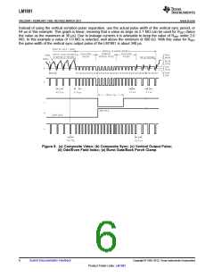
Vertical Sync Width
Burst Gate Width
190
2.5
32
µs
µs
µs
2.7 kΩ from Pin 5 to VCC
(4)
Vertical Default Time
65
(1) Typicals are at TJ = 25°C and represent the most likely parametric norm.
(2) Relative difference between the input clamp voltage and the minimum input voltage which produces a horizontal output pulse.
(3) Careful attention should be made to prevent parasitic capacitance coupling from any output pin (Pins 1, 3, 5 and 7) to the RSET pin (Pin
6).
(4) Delay time between the start of vertical sync (at input) and the vertical output pulse.
2
Submit Documentation Feedback
Copyright © 1995–2013, Texas Instruments Incorporated
Product Folder Links: LM1881

 TI [ TEXAS INSTRUMENTS ]