LF155, LF156, LF355, LF356, LF357
www.ti.com
SNOSBH0C –MAY 2000–REVISED MARCH 2013
APPLICATION HINTS
These are op amps with JFET input devices. These JFETs have large reverse breakdown voltages from gate to
source and drain eliminating the need for clamps across the inputs. Therefore large differential input voltages can
easily be accommodated without a large increase in input current. The maximum differential input voltage is
independent of the supply voltages. However, neither of the input voltages should be allowed to exceed the
negative supply as this will cause large currents to flow which can result in a destroyed unit.
Exceeding the negative common-mode limit on either input will force the output to a high state, potentially
causing a reversal of phase to the output. Exceeding the negative common-mode limit on both inputs will force
the amplifier output to a high state. In neither case does a latch occur since raising the input back within the
common-mode range again puts the input stage and thus the amplifier in a normal operating mode.
Exceeding the positive common-mode limit on a single input will not change the phase of the output however, if
both inputs exceed the limit, the output of the amplifier will be forced to a high state.
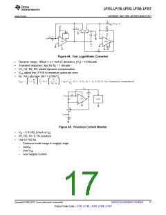
These amplifiers will operate with the common-mode input voltage equal to the positive supply. In fact, the
common-mode voltage can exceed the positive supply by approximately 100 mV independent of supply voltage
and over the full operating temperature range. The positive supply can therefore be used as a reference on an
input as, for example, in a supply current monitor and/or limiter.
Precautions should be taken to ensure that the power supply for the integrated circuit never becomes reversed in
polarity or that the unit is not inadvertently installed backwards in a socket as an unlimited current surge through
the resulting forward diode within the IC could cause fusing of the internal conductors and result in a destroyed
unit.
All of the bias currents in these amplifiers are set by FET current sources. The drain currents for the amplifiers
are therefore essentially independent of supply voltage.
As with most amplifiers, care should be taken with lead dress, component placement and supply decoupling in
order to ensure stability. For example, resistors from the output to an input should be placed with the body close
to the input to minimize “pickup” and maximize the frequency of the feedback pole by minimizing the capacitance
from the input to ground.
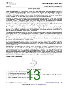
A feedback pole is created when the feedback around any amplifier is resistive. The parallel resistance and
capacitance from the input of the device (usually the inverting input) to AC ground set the frequency of the pole.
In many instances the frequency of this pole is much greater than the expected 3dB frequency of the closed loop
gain and consequently there is negligible effect on stability margin. However, if the feedback pole is less than
approximately six times the expected 3 dB frequency a lead capacitor should be placed from the output to the
input of the op amp. The value of the added capacitor should be such that the RC time constant of this capacitor
and the resistance it parallels is greater than or equal to the original feedback pole time constant.
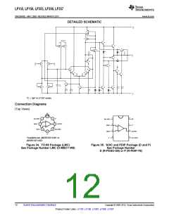
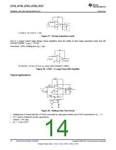
Typical Circuit Connections
Figure 36. VOS Adjustment
•
•
•
VOS is adjusted with a 25k potentiometer
The potentiometer wiper is connected to V+
For potentiometers with temperature coefficient of 100 ppm/°C or less the additional drift with adjust is ≈
0.5μV/°C/mV of adjustment
•
Typical overall drift: 5μV/°C ±(0.5μV/°C/mV of adj.)
Copyright © 2000–2013, Texas Instruments Incorporated
Submit Documentation Feedback
13
Product Folder Links: LF155 LF156 LF355 LF356 LF357

 TI [ TEXAS INSTRUMENTS ]