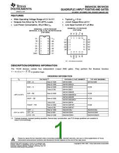
SN54HC08, SN74HC08
QUADRUPLE 2-INPUT POSITIVE-AND GATES
www.ti.com
SCLS081F–DECEMBER 1982–REVISED JANUARY 2007
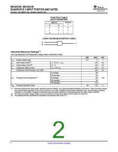
FUNCTION TABLE
(EACH INVERTER)
INPUTS
OUTPUT
Y
A
H
L
B
H
X
L
H
L
L
X
LOGIC DIAGRAM (POSITIVE LOGIC)
A
Y
B
Absolute Maximum Ratings(1)
over operating free-air temperature range (unless otherwise noted)
MIN
MAX
UNIT
V
VCC Supply voltage range
–0.5
7
±20
±20
±25
±50
86
IIK
IOK
IO
Input clamp current(2)
Output clamp current(2)
VI < 0 or VI > VCC
VO < 0
mA
mA
mA
mA
Continuous output current
Continuous current through VCCor GND
VO = 0 to VCC
D package
DB package
N package
NS package
PW package
96
θJA
Package thermal impedance(3)
80
°C/W
°C
76
113
150
Tstg
Storage temperature range
–60
(1) Stresses beyond those listed under "absolute maximum ratings" may cause permanent damage to the device. These are stress ratings
only, and functional operation of the device at these or any other conditions beyond those indicated under "recommended operating
conditions" is not implied. Exposure to absolute-maximum-rated conditions for extended periods may affect device reliability.
(2) The input and output voltage ratings may be exceeded if the input and output current ratings are observed.
(3) The package thermal impedance is calculated in accordance with JESD 51-7.
2
Submit Documentation Feedback

 TI [ TEXAS INSTRUMENTS ]