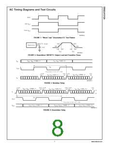
AC Timing Diagrams and Test Circuits (Continued)
DS101387-21
SW - Setup and Hold Time (Internal data sampling window)
t
t
- Serializer Output Bit Position Jitter
JIT
= Receiver Sampling Margin Time
RSM
FIGURE 9. Receiver Bus LVDS Input Skew Margin
The Deserializer noise margin is the amount of input jitter
(phase noise) that the Deserializer can tolerate and still
reliably receive data. Various environmental and systematic
factors include:
Application Information
Using the DS92LV1021 and DS92LV1212A
The Serializer and Deserializer chipset is an easy to use
transmitter and receiver pair that sends 10 bits of parallel
LVTTL data over a serial Bus LVDS link up to 660 Mbps. An
on-board PLL serializes the input data and embeds two clock
bits within the data stream. The Deserializer uses a separate
reference clock (REFCLK) and an onboard PLL to extract
the clock information from the incoming data stream and
then deserialize the data. The Deserializer monitors the
incoming clock information, determines lock status, and as-
serts the LOCK output high when loss of lock occurs.
Serializer: TCLK jitter, VCC noise (noise bandwidth and
out-of-band noise)
Media: ISI, Large VCM shifts
Deserializer: VCC noise
Recovering from LOCK Loss
In the case where the Deserializer loses lock during data
transmission, up to 3 cycles of data that were previously
received can be invalid. This is due to the delay in the lock
detection circuit. The lock detect circuit requires that invalid
clock information be received 4 times in a row to indicate
loss of lock. Since clock information has been lost, it is
possible that data was also lost during these cycles. There-
fore, after the Deserializer relocks to the incoming data
stream and the Deserializer LOCK pin goes low, at least
three previous data cycles should be suspect for bit errors.
Power Considerations
An all CMOS design of the Serializer and Deserializer makes
them inherently low power devices. In addition, the constant
current source nature of the Bus LVDS outputs minimizes
the slope of the speed vs. ICC curve of conventional CMOS
designs.
Powering Up the Deserializer
The Deserializer can relock to the incoming data stream by
making the Serializer resend SYNC patterns, as described
above, or by random locking, which can take more time,
depending on the data patterns being received.
The DS92LV1212A can be powered up at any time by fol-
lowing the proper sequence. The REFCLK input can be
running before the Deserializer powers up, and it must be
running in order for the Deserializer to lock to incoming data.
The Deserializer outputs will remain in TRI-STATE until the
Deserializer detects data transmission at its inputs and locks
to the incoming data stream.
Hot Insertion
All the BLVDS devices are hot pluggable if you follow a few
rules. When inserting, ensure the Ground pin(s) makes con-
tact first, then the VCC pin(s), and then the I/O pins. When
removing, the I/O pins should be unplugged first, then the
VCC, then the Ground. Random lock hot insertion is illus-
trated in Figure 10.
Transmitting Data
Once you power up the Serializer and Deserializer, they
must be phase locked to each other to transmit data. Phase
locking occurs when the Deserializer locks to incoming data
or when the Serializer sends patterns. The Serializer sends
SYNC patterns whenever the SYNC1 or SYNC2 inputs are
high. The LOCK output of the Deserializer remains high until
it has locked to the incoming data stream. Connecting the
LOCK output of the Deserializer to one of the SYNC inputs of
the Serializer will guarantee that enough SYNC patterns are
sent to achieve Deserializer lock.
PCB Considerations
The Bus LVDS Serializer and Deserializer should be placed
as close to the edge connector as possible. In multiple
Deserializer applications, the distance from the Deserializer
to the slot connector appears as a stub to the Serializer
driving the backplane traces. Longer stubs lower the imped-
ance of the bus, increase the load on the Serializer, and
lower the threshold margin at the Deserializers. Deserializer
devices should be placed much less than one inch from slot
connectors. Because transition times are very fast on the
Serializer Bus LVDS outputs, reducing stub lengths as much
as possible is the best method to ensure signal integrity.
The Deserializer can also lock to incoming data by simply
powering up the device and allowing the “random lock”
circuitry to find and lock to the data stream.
While the Deserializer LOCK output is low, data at the De-
serializer outputs (ROUT0-9) is valid, except for the specific
case of loss of lock during transmission which is further
discussed in the ’Recovering from LOCK Loss’ section be-
low.
Transmission Media
The Serializer and Deserializer can also be used in
point-to-point configuration of a backplane, through a PCB
trace, or through twisted pair cable. In point-to-point configu-
ration, the transmission media need only be terminated at
Noise Margin
www.national.com
10

 TI [ TEXAS INSTRUMENTS ]