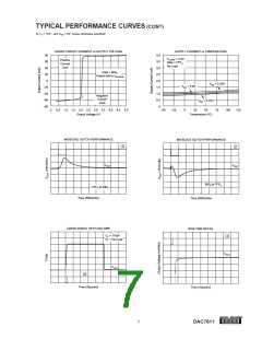
The output amplifier has a 7µs typical settling time to ±1
LSB of the final value. Note that there are differences in the
settling time for negative-going signals versus positive-
going signals.
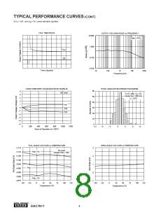
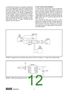
The DAC7611 power supply should be bypassed as shown
in Figure 1. The bypass capacitors should be placed as close
to the device as possible, with the 0.1uF capacitor taking
priority in this regard. The Power Supply Rejection vs
Frequency graph in the Typical Performance Curves section
shows the PSRR performance of the DAC7611. This should
be taken into account when using switching power supplies
or DC/DC converters.
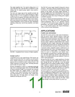
The rail-to-rail output stage of the amplifier provides the
full-scale range of 0V to 4.095V while operating on a supply
voltage as low as 4.75V. In addition to its ability to drive
resistive loads, the amplifier will remain stable while driving
capacitive loads of up to 500pF. See Figure 3 for an equiva-
lent circuit schematic of the amplifier’s output driver and the
Typical Performance Curves section for more information
regarding settling time, load driving capability, and output
noise.
In addition to offering guaranteed performance with VDD in
the 4.75V to 5.25V range, the DAC7611 will operate with
reduced performance down to 4.5V. Operation between
4.5V and 4.75V will result in longer settling time, reduced
performance, and current sourcing capability. Consult the
VDD vs Load Current graph in the Typical Performance
Curves section for more information.
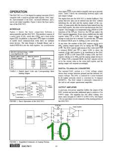
VDD
APPLICATIONS
POWER AND GROUNDING
P-Channel
The DAC7611 can be used in a wide variety of situations—
from low power, battery operated systems to large-scale
industrial process control systems. In addition, some appli-
cations require better performance than others, or are par-
ticularly sensitive to one or two specific parameters. This
diversity makes it difficult to define definite rules to follow
concerning the power supply, bypassing, and grounding.
The following discussion must be considered in relation to
the desired performance and needs of the particular system.
VOUT
N-Channel
AGND
A precision analog component requires careful layout, ad-
equate bypassing, and a clean, well-regulated power supply.
As the DAC7611 is a single-supply, +5V component, it will
often be used in conjunction with digital logic,
microcontrollers, microprocessors, and digital signal proces-
sors. The more digital logic present in the design and the
higher the switching speed, the more difficult it will be to
achieve good performance.
FIGURE 3. Simplified Driver Section of Output Amplifier.
POWER SUPPLY
A BiCMOS process and careful design of the bipolar and
CMOS sections of the DAC7611 result in a very low power
device. Bipolar transistors are used where tight matching
and low noise are needed to achieve analog accuracy, and
CMOS transistors are used for logic, switching functions
and for other low power stages.
Because the DAC7611 has a single ground pin, all return
currents, including digital and analog return currents, must
flow through this pin. The GND pin is also the ground
reference point for the internal bandgap reference. Ideally,
GND would be connected directly to an analog ground
plane. This plane would be separate from the ground con-
nection for the digital components until they are connected
at the power entry point of the system (see Figure 4).
If power consumption is critical, it is important to keep the
logic levels on the digital inputs (SDI, CLK, CS, LD, CLR)
as close as possible to either VDD or ground. This will keep
the CMOS inputs (see “Supply Current vs Logic Input
Voltages” in the Typical Performance Curves) from shunt-
ing current between VDD and ground. Thus, CMOS logic
levels rather than TTL logic levels, are strongly recom-
mended for driving the DAC7611.
The power applied to VDD should be well regulated and low-
noise. Switching power supplies and DC/DC converters will
often have high-frequency glitches or spikes riding on the
output voltage. In addition, digital components can create
similar high frequency spikes as their internal logic switches
states. This noise can easily couple into the DAC output
voltage through various paths between VDD and VOUT
.
®
11
DAC7611

 TI [ TEXAS INSTRUMENTS ]