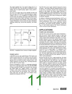
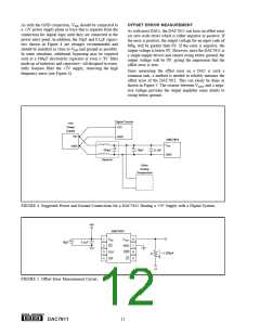
As with the GND connection, VDD should be connected to
a +5V power supply plane or trace that is separate from the
connection for digital logic until they are connected at the
power entry point. In addition, the 10µF and 0.1µF capaci-
tors shown in Figure 4 are strongly recommended and
should be installed as close to VDD and ground as possible.
In some situations, additional bypassing may be required
such as a 100µF electrolytic capacitor or even a “Pi” filter
made up of inductors and capacitors—all designed to essen-
tially lowpass filter the +5V supply, removing the high
frequency noise (see Figure 4).
OFFSET ERROR MEASUREMENT
As with most DACs, the DAC7611 can have an offset error
(or zero scale error) which is either negative or positive. If
the error is positive, the output voltage for an input code of
000H will be greater than 0V. If the error is negative, the
output voltage is below 0V. However, since the DAC7611 is
a single-supply device and cannot swing below ground, the
output voltage will be 0V, giving the impression that the
offset error is zero.
Since measuring the offset error on a DAC is such a
common task, a method is needed to reliably measure the
offset error of the DAC7611. This can easily be done as
shown in Figure 5. The resistor between VOUT and a nega-
tive voltage provides the output amplifier some ability to
swing below ground.
Digital Circuits
+5V
Power
Supply
+5V
+5V
GND
DAC7611
VDD
GND
+
+
100µF
10µF
0.1µF
GND
Optional
Other
Analog
Components
FIGURE 4. Suggested Power and Ground Connections for a DAC7611 Sharing a +5V Supply with a Digital System.
+5V
DAC7611
1
2
3
4
VDD
CS
VOUT
GND
CLR
LD
8
7
6
5
+
10µF
0.1µF
CLK
SDI
i ≤ 200µA
R
–V
FIGURE 5. Offset Error Measurement Circuit.
®
12
DAC7611

 TI [ TEXAS INSTRUMENTS ]