clear input (CLR) is provided to simplify start-up or periodic
resets. Table I shows the relationship between input code
and output voltage.
OPERATION
The DAC7611 is a 12-bit digital-to-analog converter (DAC)
complete with a serial-to-parallel shift register, DAC regis-
ter, laser-trimmed 12-bit DAC, on-board reference, and a
rail-to-rail output amplifier. Figure 1 shows the basic opera-
tion of the DAC7611.
The digital data into the DAC7611 is double-buffered. This
means that new data can be entered into the DAC without
disturbing the old data and the analog output of the con-
verter. At some point after the data has been entered into the
serial shift register, this data can be transferred into the DAC
register. This transfer is accomplished with a HIGH to LOW
transition of the LD pin. However, the LD pin makes the
DAC register transparent. If new data is shifted into the shift
register while LD is LOW, the DAC output voltage will
change as each new bit is entered. To prevent this, LD must
be returned HIGH prior to shifting in new serial data.
INTERFACE
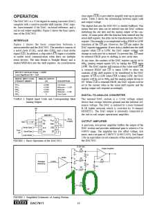
Figure 1 shows the basic connection between a
microcontroller and the DAC7611. The interface consists of
a serial clock (CLK), serial data (SDI), and a load strobe
signal (LD). In addition, a chip select (CS) input is available
to enable serial communication when there are multiple
serial devices. The data format is Straight Binary and is
loaded MSB-first into the shift registers. An asynchronous
At any time, the contents of the DAC register can be set to
000H (analog output equals 0V) by taking the CLR input
LOW. The DAC register will remain at this value until CLR
is returned HIGH and LD is taken LOW to allow the
contents of the shift register to be transferred to the DAC
register. If LD is LOW when CLR is taken LOW, the DAC
register will be set to 000H and the analog output driven to
0V. When CLR is returned HIGH, the DAC register will be
set to the current value in the serial shift register and the
analog output will respond accordingly.
DAC7611 Full-Scale Range = 4.095V
Least Significant Bit = 1mV
DIGITAL INPUT CODE
STRAIGHT BINARY
ANALOG OUTPUT
(V)
DESCRIPTION
FFFH
801H
800H
7FFH
000H
+4.095
+2.049
+2.048
+2.047
0
Full Scale
Midscale + 1 LSB
Midscale
Midscale – 1 LSB
Zero Scale
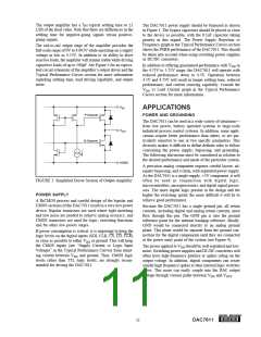
DIGITAL-TO-ANALOG CONVERTER
TABLE I. Digital Input Code and Corresponding Ideal
Analog Output.
The internal DAC section is a 12-bit voltage output
device that swings between ground and the internal ref-
erence voltage. The DAC is realized by a laser-trimmed
R-2R ladder network which is switched by N-channel
MOSFETs. The DAC output is internally connected to
the rail-to-rail output operational amplifier.
+5V
DAC7611
0V to
+4.095V
1
2
3
4
VDD
CS
VOUT
GND
CLR
LD
8
7
6
5
+
OUTPUT AMPLIFIER
10µF
0.1µF
A precision, low-power amplifier buffers the output of the
DAC section and provides additional gain to achieve a 0 to
4.095V range. The amplifier has low offset voltage, low
noise, and a set gain of 1.682V/V (4.095/2.435). See Figure
2 for an equivalent circuit schematic of the analog portion of
the DAC7611.
Serial Clock
Serial Data
Load Strobe
CLK
SDI
From
µC
FIGURE 1. Basic Operation of the DAC7611.
R-2R DAC
Output Amplifier
2R
2R
2R
R
Buffer
R2
Bandgap
2.435V
Reference
R
R
R1
2R
2R
FIGURE 2. Simplified Schematic of Analog Portion.
®
10
DAC7611

 TI [ TEXAS INSTRUMENTS ]