CC2510Fx / CC2511Fx
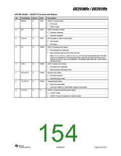
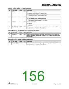
U0GCR (0xC5) - USART 0 Generic Control
Bit
Field Name
Reset
R/W
Description
7
CPOL
0
R/W
SPI 0 clock polarity
0
1
Negative clock polarity (SCK low when idle)
Positive clock polarity (SCK high when idle)
6
CPHA
0
R/W
R/W
R/W
SPI 0 clock phase
0
1
Data centered on first edge of SCK period
Data centered on second edge of SCK period
5
ORDER
0
Bit order for transfers
0
1
LSB first
MSB first
4:0
BAUD_E[4:0]
00000
Baud rate exponent value. BAUD_Ealong with BAUD_Mdecides the UART 0
baud rate and the SPI 0 clock (SCK) frequency
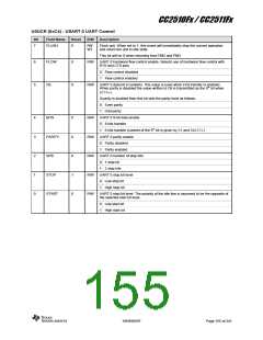
U0DBUF (0xC1) - USART 0 Receive/Transmit Data Buffer
Bit
Field Name
Reset
R/W
Description
7:0
DATA[7:0]
0x00
R/W
USART 0 receive and transmit data buffer. Writing data to U0DBUFplaces the
data into the internal transmit buffer. Reading U0DBUFreturns the contents of the
receive buffer.
U0BAUD (0xC2) - USART 0 Baud Rate Control
Bit
Field Name
Reset
R/W
Description
7:0
BAUD_M[7:0]
0x00
R/W
Baud rate mantissa value. BAUD_Malong with BAUD_Edecides the UART 0
baud rate and the SPI 0 clock (SCK) frequency
SWRS055F
Page 156 of 241

 TI [ TEXAS INSTRUMENTS ]