CC2510Fx / CC2511Fx
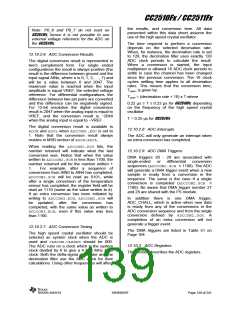
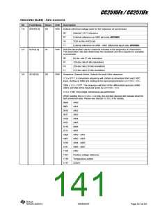
ADCCON2 (0xB5) - ADC Control 2
Bit
Field Name
Reset
R/W
Description
Selects reference voltage used for the sequence of conversions
7:6
SREF[1:0]
00
R/W
00
01
10
11
Internal 1.25 V reference
External reference on AIN7 pin (only CC2510Fx)
VDD on the AVDD pin
External reference on AIN6 - AIN7 differential input (only CC2510Fx)
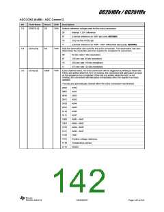
5:4
SDIV[1:0]
01
R/W
Sets the decimation rate for channels included in the sequence of conversions.
The decimation rate also determines the resolution and time required to complete
a conversion.
00
01
10
11
64 dec rate (7 bits resolution)
128 dec rate (9 bits resolution)
256 dec rate (10 bits resolution)
512 dec rate (12 bits resolution)
3:0
SCH[3:0]
00
R/W
Sequence Channel Select. Selects the end of the sequence.
SCH≤ 0111: A conversion sequence will contain a conversion from each ADC
input, starting at AIN0 and ending at the input programmed in ADCCON2.SCH.
1000 ≤ SCH≤ 1011: The sequence will start at the differential input pair (AIN0 -
AIN1) and stop at the input pair given by ADCCON2.SCH.
SCH≥ 1100: Only single conversions are performed.
When reading the ADCCON2.SCHbits, the number returned will indicate what the
last conversion was. Please see Section 12.10.2.6 for details.
0000
0001
0010
0011
0100
0101
0110
0111
1000
1001
1010
1011
1100
1101
1110
1111
AIN0
AIN1
AIN2
AIN3
AIN4
AIN5
AIN6
AIN7
AIN0 - AIN1
AIN2 - AIN3
AIN4 - AIN5
AIN6 - AIN7
GND
Positive voltage reference
Temperature sensor
VDD/3
SWRS055F
Page 141 of 241

 TI [ TEXAS INSTRUMENTS ]