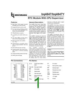
bq4847/bq4847Y
room temperature. For a complete description of fea-
tures, operating conditions, electrical characteristics,
bus timing, and pin descriptions, see the bq4845 data
sheet. Valid part types for ordering are bq4847MT (5%)
and bq4847YMT (10%).
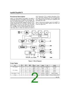
Functional Description
Figure 1 is a block diagram of the bq4847. The bq4847 is
functionally equivalent to the bq4845 except that the bat-
tery (20, 24) and crystal (2, 3) pins are not accessible. The
pins are connected internally to a coin cell and quartz
crystal. The coin cell provides 130mAh of capacity. It is in-
ternally isolated from VOUT and CEOUT until the initial
application of VCC. Once VCC rises above VPFD, this isola-
tion is broken, and the backup cell provides power to
VOUT and CEOUT for the external SRAM. The real-time
clock keeps time to within one minute per month at
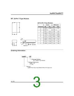
Figure 2 illustrates the address map for the bq4847. Ta-
ble 1 is a map of the bq4847 registers, and Table 2 de-
scribes the register bits.
Figure 1. Block Diagram
Truth Table
VCC
CS
VIH
VIL
VIL
VIL
X
OE
X
WE
X
CEOUT
CEIN
CEIN
CEIN
CEIN
VOH
VOUT
VOUT1
VOUT1
VOUT1
VOUT1
VOUT1
VOUT2
Mode
Deselect
Write
DQ
Power
Standby
Active
< VCC (max.)
High Z
DIN
X
VIL
VIH
VIH
X
> VCC (min.)
VIL
VIH
X
Read
DOUT
High Z
High Z
Active
Read
Active
< VPFD (min.) > VSO
Deselect
Deselect
CMOS standby
X
X
X
VOHB
High Z Battery-backup mode
≤ VSO
Sept. 1996
2

 TI [ TEXAS INSTRUMENTS ]