bq4285E/L
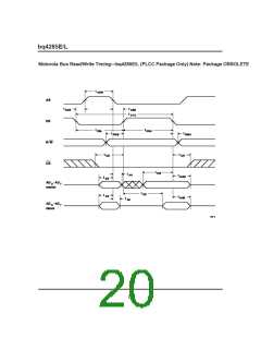
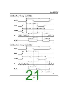
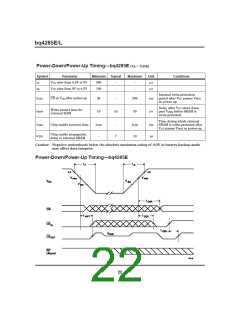
Power-Down/Power-Up Timing—bq4285E (T = T
)
OPR
A
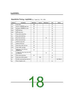
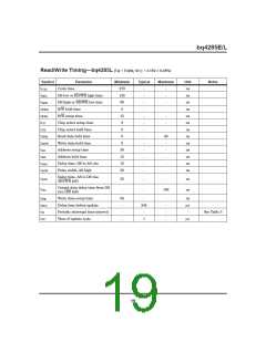
Symbol
Parameter
Minimum
300
Typical
Maximum
Unit
Conditions
tF
tR
VCC slew from 4.5V to 0V
VCC slew from 0V to 4.5V
-
-
-
-
µs
µs
100
Internal write-protection
period after VCC passes VPFD
on power-up.
tCSR
CS at VIH after power-up
20
10
-
200
30
ms
Delay after VCC slows down
past VPFD before SRAM is
write-protected.
Write-protect time for
external RAM
µs
tWPT
16
Time during which external
SRAM is write-protected after
VCC passes VPFD on power-up.
tCER
tCSR
tCSR
Chip enable recovery time
-
ms
ns
Chip enable propagation
delay to external SRAM
tCED
-
7
10
Caution: Negative undershoots below the absolute maximum rating of -0.3V in battery-backup mode
may affect data integrity.
Power-Down/Power-Up Timing—bq4285E
22

 TI [ TEXAS INSTRUMENTS ]