ꢀ ꢁ ꢂ ꢃꢄ ꢅ ꢂꢆ ꢀ ꢁ ꢂ ꢃꢄꢅ ꢇ
SLUS553D − MAY 2003 − REVISED JULY 2005
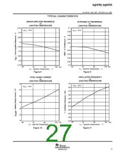
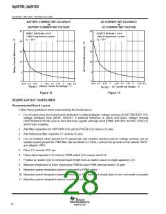
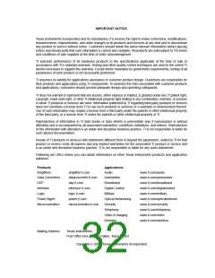
BATTERY CURRENT SET ACCURACY
AC CURRENT SET ACCURACY
vs
vs
BATTERY CURRENT SET VOLTAGE
AC CURRENT SET VOLTAGE
25
20
15
10
25
20
15
10
ACSET Full Scale = 2.5 V
SRSET Full Scale = 2.5 V
= Max Programmed Current
= Max Programmed Current
T
J
= 25°C
T
J
= 25°C
5
0
5
0
0.25 0.5 0.75
1
1.25 1.5 1.75
2
2.25 2.5
0.25 0.5 0.75
1
1.25 1.5 1.75
2
2.25 2.5
V
− Battery Current Set Voltage − V
SRSET
V
ACSET
− AC Current Set Voltage − V
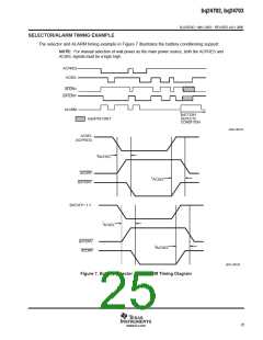
Figure 12
Figure 13
BOARD LAYOUT GUIDELINES
Recommended Board Layout
Follow these guidelines when implementing the board layout:
1. Do not place lines and components dedicated to battery/adapter voltage sensing (ACDET,BATDEP, VS),
voltage feedback loop (BATP, BATSET if external reference is used) and shunt voltage sensing
(SRP/SRN/ACP/ACN) close to lines that have signals with high dv/dt (PWM, BATDRV, ACDRV, VHSP) to
avoid noise coupling.
2. Add filter capacitors for SRP/SRN (C8) and ACP/ACN (C3) close to IC pins
3. Add Reference filter capacitor C1 close to IC pins
4. Use an isolated, clean ground for IC ground pin and resistive dividers used in voltage sensing; use an
isolated power ground for PWM filter cap and diode (C11/D4). Connect the grounds to the battery PACK−
and adapter GND.
5. Place C7 close to VCC pin.
6. Place input capacitor C12 close to PWM switch (U3) source and R14.
7. Position ac switch (U2) to minimize trace length from ac switch source to input capacitor C12.
8. Minimize inductance of trace connecting PWM pin and PWM external switch U3 gate
9. Maximize power dissipation planes connected to PWM switch
10. Maximize power dissipation planes connected to SRP resistor if steady state in zero volt mode is possible
11. Maximize power dissipation planes connected to D1
28
www.ti.com

 TI [ TEXAS INSTRUMENTS ]