bq24296
bq24297
www.ti.com
SLUSBP6A –SEPTEMBER 2013–REVISED OCTOBER 2013
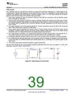
PCB Layout
The switching node rise and fall times should be minimized for minimum switching loss. Proper layout of the
components to minimize high frequency current path loop (see Figure 42) is important to prevent electrical and
magnetic field radiation and high frequency resonant problems. Here is a PCB layout priority list for proper
layout. Layout PCB according to this specific order is essential.
1. Place input capacitor as close as possible to PMID pin and GND pin connections and use shortest copper
trace connection or GND plane.
2. Place inductor input terminal to SW pin as close as possible. Minimize the copper area of this trace to lower
electrical and magnetic field radiation but make the trace wide enough to carry the charging current. Do not
use multiple layers in parallel for this connection. Minimize parasitic capacitance from this area to any other
trace or plane.
3. Put output capacitor near to the inductor and the IC. Ground connections need to be tied to the IC ground
with a short copper trace connection or GND plane.
4. Route analog ground separately from power ground. Connect analog ground and connect power ground
separately. Connect analog ground and power ground together using power pad as the single ground
connection point. Or using a 0Ω resistor to tie analog ground to power ground.
5. Use single ground connection to tie charger power ground to charger analog ground. Just beneath the IC.
Use ground copper pour but avoid power pins to reduce inductive and capacitive noise coupling.
6. Decoupling capacitors should be placed next to the IC pins and make trace connection as short as possible.
7. It is critical that the exposed power pad on the backside of the IC package be soldered to the PCB ground.
Ensure that there are sufficient thermal vias directly under the IC, connecting to the ground plane on the
other layers.
8. The via size and number should be enough for a given current path.
See the EVM design for the recommended component placement with trace and via locations. For the QFN
information, refer to SCBA017 and SLUA271.
Figure 42. High Frequency Current Path
Copyright © 2013, Texas Instruments Incorporated
Submit Documentation Feedback
39
Product Folder Links: bq24296 bq24297

 TI [ TEXAS INSTRUMENTS ]