bq20z80-V101
www.ti.com
SLUS625D–SEPTEMBER 2004–REVISED OCTOBER 2005
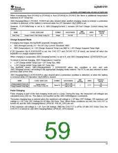
bq20z80 Normal
Charging Mode
(CHG FET = ON)
Turn CHG FET on
Reset t
Timer
TERM
and Start t
MAX
Hold
Timer
t
CHG_OFF
No
Timer
Turn CHG FET off,
Yes
Is V
Has t
CELLMAX
MAX
Reset t
CHG_ON
< V
?
expired?
CHG_ON
Timer
Yes
No
Yes
No
No
Has t
CHG_ON
Yes
Has I
TERM
Is V
CELLMAX
Yes
Reset
expired?
No
Been Reached?
(Normal charge
termination)
Has t
t
> V
MAX
?
CHG_OFF
CHG_OFF
expired?
Timer
No
Yes
No
Is V
Yes
Reset and Start
CELLMAX
Set Terminate Charge
Alarm
t
Timer
> V
CHG_OFF
?
CHG_ON
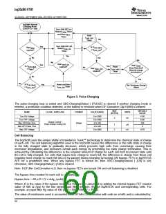
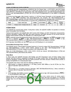
Figure 3. Pulse Charging
The pulse-charging loop is exited and SBS.ChargingStatus( ) [PULSE] is cleared if another charging mode is
entered, a protection condition detected, or the battery is removed when DF:Operation Cfg B [NR] is cleared.
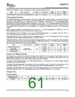
SIZE
(BYTES)
DEFAULT
VALUE
NAME
CLASS / SUBCLASS
FORMAT
VALID RANGE
UNITS
Turn ON Voltage
Turn OFF Voltage
Max ON Pulse Time
Max OFF Pulse Time
Max OFF Voltage
0 to 5000
0 to 5000
0 to 240
0 to 240
0 to 5000
4150
4250
240
0
2
mV
Charge Control /
Pulse Charge Config (35)
Integer
1
2
s/4
mV
4270
Cell Balancing
The bq20z80 uses the unique ability of Impedance Track™ technology to determine the chemical state of charge
of each cell. The cell balancing algorithm used in the bq20z80 causes the differences in the cells state of charge
in the fully charged state to gradually decrease, which prevents high cells from overcharge causing their
excessive degradation, and increases overall pack energy by preventing too early charge termination. This is
achieved by calculating the differences in the required amount of charge for each cell from its present state until
the cell is fully charged. For cells that require less charge to reach full, the difference in charge from those cell
requiring more charge to reach full (dQ) is by-passed during charging by turning ON bypass FETs in bq29312A
AFE for a predefined time. When any bypass FET is turned on, then SBS.ChargingStatus( ) [CB] is set;
otherwise, SBS.ChargingStatus( ) [CB] is cleared.
Note: If DF:Min Cell Deviation is 0, then no bypass FETs are turned ON and cell balancing is disabled.
The bypass time needed for each cell is calculated as
Bypass time = dQ x R / (V x duty_cycle).
Where, R is the value of the bypass resistance that can be calculated by adding the internal bypass FET resistor
value of 500 Ω (typ) to the two series input filter resistors (Rχ) of bq29312A and corresponding cells. For
example: an input filter Rχ value of 100 Ω, R = 500 +100 x 2 = 700 Ω.
The value of resistances used is accounted for in DF:Min Cell Deviation with units on s/mAh and is calculated by:
60

 TI [ TEXAS INSTRUMENTS ]