AM26C31C, AM26C31I, AM26C31M
QUADRUPLE DIFFERENTIAL LINE DRIVERS
SLLS103G – DECEMBER 1990 – REVISED SEPTEMBER 1998
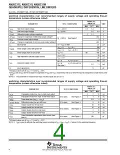
electrical characteristics over recommended ranges of supply voltage and operating free-air
temperature (unless otherwise noted)
AM26C31M
PARAMETER
TEST CONDITIONS
UNIT
†
MIN TYP
MAX
V
V
High-level output voltage
I
I
= –20 mA
= 20 mA
2.2
3.4
0.2
3.1
V
V
V
OH
O
Low-level output voltage
0.4
OL
O
|V
|
Differential output voltage magnitude
2
OD
Change in magnitude of differential
output voltage
∆|V
|
|
±0.4
3
V
V
OD
‡
R
= 100 Ω, See Figure 1
L
V
OC
Common-mode output voltage
Change in magnitude of common-mode
∆|V
±0.4
V
OC
‡
output voltage
I
I
I
I
Input current
V = V or GND
CC
±1
100
–100
–170
20
µA
I
I
V
V
V
V
V
= 0,
= 0,
V
= 6 V
CC
O
O
Driver output current with power off
Driver output short-circuit current
High-impedance off-state output current
µA
O(off)
OS
V
= –0.25 V
CC
= 0
mA
µA
µA
µA
mA
pF
O
O
O
= 2.5 V
= 0.5 V
OZ
–20
100
3.2
I
I
= 0,
= 0,
V = 0 V or 5 V
I
O
I
Quiescent supply current
Input capacitance
CC
V = 2.4 V or 0.5 V, See Note 2
I
O
C
6
i
†
‡
All typical values are at V
= 5 V and T = 25°C.
A
CC
∆|V
| and ∆|V
OD
| are the changes in magnitude of V
OC OD
and V
, respectively, that occur when the input is changed from a high level to a low
OC
level.
NOTE 2: This parameter is measured per input. All other inputs are at 0 V or 5 V.
switching characteristics over recommended ranges of supply voltage and operating free-air
temperature (unless otherwise noted)
AM26C31M
PARAMETER
TEST CONDITIONS
UNIT
†
MIN TYP
MAX
12
t
t
t
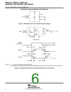
Propagation delay time, low- to high-level output
Propagation delay time, high- to low-level output
7
ns
ns
ns
PLH
PHL
sk(p)
S1 is open,
See Figure 2
See Figure 3
6.5
0.5
12
Pulse skew time (|t
– t
|)
4
PLH PHL
t
t
t
t
t
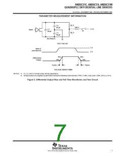
, t
Differential output rise and fall times
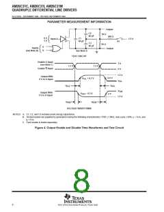
Output enable time to high level
Output enable time to low level
Output disable time from high level
Output disable time from low level
S1 is open,
5
10
10
7
12
19
19
16
16
ns
ns
ns
ns
ns
r(OD) f(OD)
PZH
PZL
S1 is closed,
See Figure 4
See Figure 2
PHZ
7
PLZ
Power dissipation capacitance (each driver) (see
Note 3)
C
S1 is open,
100
pF
pd
†
All typical values are at V
= 5 V and T = 25°C.
A
CC
is used to estimate the switching losses according to P = C × V
2
× f, where f is the switching frequency.
CC
NOTE 3:
C
pd
D
pd
5
POST OFFICE BOX 655303 • DALLAS, TEXAS 75265

 TI [ TEXAS INSTRUMENTS ]