ADS7056
www.ti.com.cn
ZHCSG66 –MARCH 2017
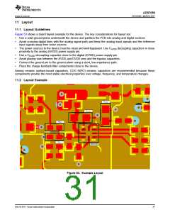
11 Layout
11.1 Layout Guidelines
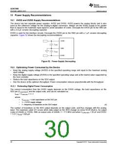
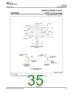
Figure 53 shows a board layout example for the device. The key considerations for layout are:
•
•
Use a solid ground plane underneath the device and partition the PCB into analog and digital sections
Avoid crossing digital lines with the analog signal path and keep the analog input signals and the reference
input signals away from noise sources.
•
The power sources to the device must be clean and well-bypassed. Use CAVDD decoupling capacitors in close
proximity to the analog (AVDD) power supply pin.
•
•
•
•
Use a CDVDD decoupling capacitor close to the digital (DVDD) power-supply pin.
Avoid placing vias between the AVDD and DVDD pins and the bypass capacitors.
Connect the ground pin to the ground plane using a short, low-impedance path.
Place the charge kickback filter components close to the device.
Among ceramic surface-mount capacitors, COG (NPO) ceramic capacitors are recommended because these
components provide the most stable electrical properties over voltage, frequency, and temperature changes.
11.2 Layout Example
Figure 53. Example Layout
版权 © 2017, Texas Instruments Incorporated
31

 TI [ TEXAS INSTRUMENTS ]