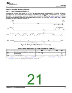
ADS7056
www.ti.com.cn
ZHCSG66 –MARCH 2017
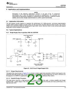
Typical Applications (continued)
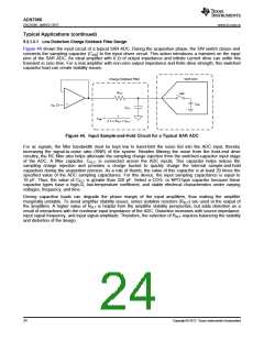
9.2.1.2.2 Input Amplifier Selection
Selection criteria for the input amplifiers is highly dependent on the input signal type as well as the performance
goals of the data acquisition system. Some key amplifier specifications to consider when selecting an appropriate
amplifier to drive the inputs of the ADC are:
•
Small-signal bandwidth: select the small-signal bandwidth of the input amplifiers to be as high as possible
after meeting the power budget of the system. Higher bandwidth reduces the closed-loop output impedance
of the amplifier, thus allowing the amplifier to more easily drive the low cutoff frequency RC filter (see the Low
Distortion Charge Kickback Filter Design section for details.) at the inputs of the ADC. Higher bandwidth also
minimizes the harmonic distortion at higher input frequencies. Select the amplifier with the unity-gain
bandwidth (UGB) as described in Equation 2 to maintain the overall stability of the input driver circuit.
1
UGB í 4ì
2Œ ìRFLT ì CFLT
where:
•
UGB = unity-gain bandwidth
(2)
•
Noise: noise contribution of the front-end amplifiers must be as low as possible to prevent any degradation in
SNR performance of the system. Generally, to ensure that the noise performance of the data acquisition
system is not limited by the front-end circuit, the total noise contribution from the front-end circuit must be
kept below 20% of the input-referred noise of the ADC. As Equation 3 explains, noise from the input driver
circuit is band limited by designing a low cutoff frequency RC filter.
SNR(dB)
-
(
)
2
1
5
VREF
2 2
V1 f _AMP_PP
Œ
20
NG ì
+e2n_RMS ì ìf
Ç
ì
ì 10
-3dB
6.6
2
where:
•
•
•
•
V1/f_AMP_PP is the peak-to-peak flicker noise in µVRMS
en_RMS is the amplifier broadband noise
f–3dB is the –3-dB bandwidth of the RC filter and
NG is the noise gain of the front-end circuit, which is equal to 1 in the buffer configuration
(3)
•
Distortion: both the ADC and the input driver introduce distortion in a data acquisition block. To ensure that
the distortion performance of the data acquisition system is not limited by the front-end circuit, the distortion of
the input driver must be at least 10 dB lower than the distortion of the ADC.
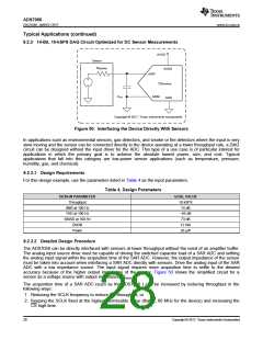
For the application circuit of Figure 43, the OPA836 is selected for its high bandwidth (205 MHz), low noise
(4.6 nV/√Hz), high output drive capacity (45 mA), and fast settling response (22 ns for 0.1% settling).
9.2.1.2.3 Reference Circuit
The analog supply voltage of the device is also used as a voltage reference for conversion. Decouple the AVDD
pin with a 3.3-µF, low-ESR ceramic capacitor.
Copyright © 2017, Texas Instruments Incorporated
25

 TI [ TEXAS INSTRUMENTS ]