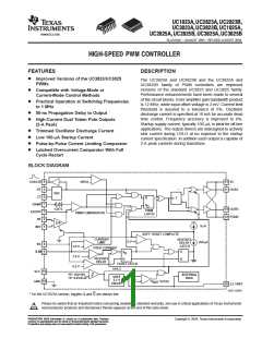
ꢀꢁꢂ ꢃ ꢄ ꢅ ꢆꢇ ꢀꢁꢄ ꢃ ꢄ ꢅ ꢆꢇ ꢀ ꢁꢄ ꢃꢄ ꢅꢈ ꢇ
ꢀꢁꢅ ꢃ ꢄ ꢅ ꢆꢇ ꢀꢁꢅ ꢃ ꢄ ꢅ ꢈꢇ ꢀ ꢁꢂ ꢃꢄ ꢉꢆ ꢇ
www.ti.com
ꢀꢁꢄ ꢃ ꢄ ꢉ ꢆꢇ ꢀꢁꢄ ꢃ ꢄ ꢉ ꢈꢇ ꢀꢁꢅ ꢃ ꢄ ꢉ ꢆꢇ ꢀ ꢁꢅ ꢃꢄ ꢉꢈ
SLUS334C − AUGUST 1995 − REVISED AUGUST 2004
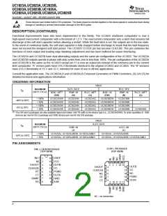
TERMINAL FUNCTIONS
TERMINAL
NO.
I/O
DESCRIPTION
NAME
J or DW
Q or L
CLK/LEB
CT
4
5
O
I
Output of the internal oscillator
Timing capacitor connection pin for oscillator frequency programming. The timing capacitor should
be connected to the device ground using minimal trace length.
6
8
EAOUT
GND
ILIM
3
10
9
4
O
−
I
Output of the error amplifier for compensation
Analog ground return pin
13
12
2
Input to the current limit comparator
INV
1
I
Inverting input to the error amplifier
NI
2
3
I
Non-inverting input to the error amplifier
High current totem pole output A of the on-chip drive stage.
High current totem pole output B of the on-chip drive stage.
Ground return pin for the output driver stage
OUTA
OUTB
PGND
11
14
12
14
18
15
O
O
−
Non-inverting input to the PWM comparator with 1.25-V internal input offset. In voltage mode
operation, this serves as the input voltage feed-forward function by using the CT ramp. In peak
current mode operation, this serves as the slope compensation input.
RAMP
7
9
I
RT
SS
5
8
7
I
I
Timing resistor connection pin for oscillator frequency programming
Soft-start input pin which also doubles as the maximum duty cycle clamp.
10
Power supply pin for the output stage. This pin should be bypassed with a 0.1-µF monolithic ceramic
low ESL capacitor with minimal trace lengths.
VC
13
15
16
17
19
20
−
−
Power supply pin for the device. This pin should be bypassed with a 0.1-µF monolithic ceramic low
ESL capacitor with minimal trace lengths
VCC
VREF
5.1-V reference. For stability, the reference should be bypassed with a 0.1-µF monolithic ceramic
low ESL capacitor and minimal trace length to the ground plane.
O
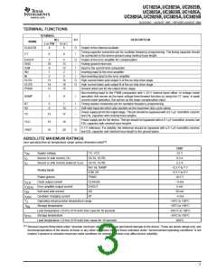
ABSOLUTE MAXIMUM RATINGS
over operating free-air temperature range unless otherwise noted
(1)
UNIT
22 V
V
IN
Supply voltage,
VC, VCC
I
I
Source or sink current, DC
Source or sink current, pulse (0.5 µs)
OUTA, OUTB
OUTA, OUTB
INV, NI, RAMP
ILIM, SS
PGND
0.5 A
O
2.2 A
O
−0.3 V to 7 V
−0.3 V to 6 V
0.2 V
Analog inputs
Power ground
I
I
I
I
Clock output current
Error amplifier output current
Soft-start sink current
Oscillator charging current
CLK/LEB
EAOUT
−5 mA
CLK
O(EA)
SS
5 mA
SS
20 mA
RT
−5 mA
OSC
T
Operating virtual junction temperature range
Storage temperature
−55°C to 150°C
−65°C to 150°C
−55C°C to 150°C
−65°C to 150°C
300°C
J
T
stg
Lead temperature 1,6 mm (1/16 inch) from case for 10 seconds
Storage temperature
t
STG
Lead temperature 1,6 mm (1/16 inch) from cases for 10 seconds
(1)
Stresses beyond those listed under “absolute maximum ratings” may cause permanent damage to the device. These are stress ratings only, and
functional operation of the device at these or any other conditions beyond those indicated under “recommended operating conditions” is not
implied. Exposure to absolute-maximum-rated conditions for extended periods may affect device reliability.
3

 TI [ TEXAS INSTRUMENTS ]