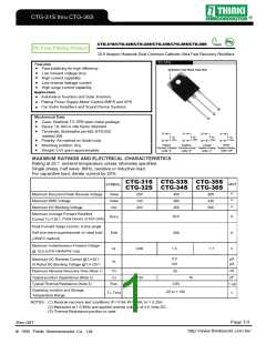
CTG-31S thru CTG-36S
Pb
CTG-31S/CTG-32S/CTG-33S/CTG-34S/CTG-35S/CTG-36S
Pb Free Plating Product
20.0 Ampere Heatsink Dual Common Cathode Ultra Fast Recovery Rectifiers
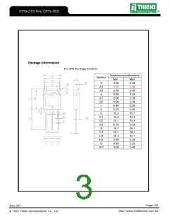
TO-3PN
Features
ꢀ
ꢀ
ꢀ
ꢀ
ꢀ
Fast switching for high efficiency
Low forward voltage drop
High current capability
Bottom Side Metal Heat Sink
Low reverse leakage current
High surge current capability
Application
Automotive Inverters and Solar Inverters
ꢀ
ꢀ
ꢀ
Plating Power Supply,Motor Control,SMPS and UPS
Car Audio Amplifiers and Sound Device Systems
Mechanical Data
ꢀ
ꢀ
ꢀ
Case: Heatsink TO-3PN open metal package
Epoxy: UL 94V-0 rate flame retardant
Terminals: Solderable per MIL-STD-202
method 208
Case
Case
Case
Case
Series
ꢀ
ꢀ
ꢀ
Polarity: As marked on diode body
Mounting position: Any
Weight: 0.61 gram approximately
Doubler
Common Cathode Common Anode Tandem Polarity Tandem Polarity
Suffix "UR"
Negative
Positive
Suffix "S"
Suffix "R"
Suffix "U"
MAXIMUM RATINGS AND ELECTRICAL CHARACTERISTICS
℃
Rating at 25 ambient temperature unless otherwise specified.
Single phase, half wave, 60Hz, resistive or inductive load.
For capacitive load, derate current by 20%.
CTG-33S CTG-35S
CTG-34S CTG-36S
CTG-31S
UNIT
SYMBOL
CTG-32S
V
V
V
Maximum Recurrent Peak Reverse Voltage
Maximum RMS Voltage
V
RRM
RMS
200
140
200
400
280
400
600
420
600
V
Maximum DC Blocking Voltage
V
DC
Maximum Average Forward Rectified
20.0
200
1.3
A
A
V
IF(AV)
℃
(Total Device 2x10A=20A)
Current TC
=125
Peak Forward Surge Current, 8.3ms single
Half sine-wave superimposed on rated load
(JEDEC method)
I
FSM
Maximum Instantaneous Forward Voltage
V
F
0.98
120
1.7
(Per Diode/Per Leg)
@ 10.0 A
5.0
100
μA
μA
Maximum DC Reverse Current @T
At Rated DC Blocking Voltage @T
J
=25
℃
℃
I
R
J
=125
nS
pF
Maximum Reverse Recovery Time (Note 1)
Typical junction Capacitance (Note 2)
Typical Thermal Resistance (Note 3)
Trr
35
C
J
70
R
JC
0.85
℃
/W
Operating Junction and Storage
Temperature Range
-55 to + 150
℃
T , TSTG
J
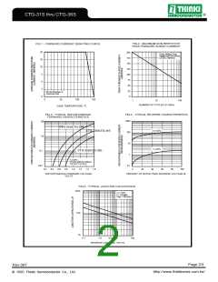
NOTES : (1) Reverse recovery test conditions IF= 0.5A, IR= 1.0A, Irr = 0.25A.
(2) Measured at 1.0 MHz and applied reverse voltage of 4.0 Volts DC.
(3) Thermal Resistance junction to case.
Page 1/3
http://www.thinkisemi.com.tw/
Rev.08T
© 1995 Thinki Semiconductor Co., Ltd.

 THINKISEMI [ Thinki Semiconductor Co., Ltd. ]