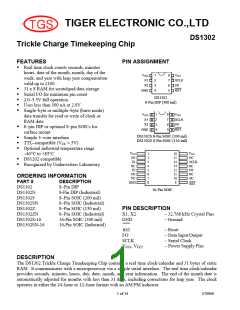
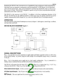
DS1302
X1, X2 – Connections for a standard 32.768 kHz quartz crystal. The internal oscillator is designed for
operation with a crystal having a specified load capacitance of 6 pF. For more information on crystal
selection and crystal layout considerations, please consult Application Note 58, “Crystal Considerations
with Real Time Clocks.” The DS1302 can also be driven by an external 32.768 kHz oscillator. In
this configuration, the X1 pin is connected to the external oscillator signal and the X2 pin is floated.
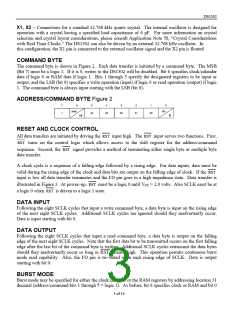
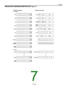
COMMAND BYTE
The command byte is shown in Figure 2. Each data transfer is initiated by a command byte. The MSB
(Bit 7) must be a logic 1. If it is 0, writes to the DS1302 will be disabled. Bit 6 specifies clock/calendar
data if logic 0 or RAM data if logic 1. Bits 1 through 5 specify the designated registers to be input or
output, and the LSB (bit 0) specifies a write operation (input) if logic 0 or read operation (output) if logic
1. The command byte is always input starting with the LSB (bit 0).
ADDRESS/COMMAND BYTE Figure 2
RESET AND CLOCK CONTROL
All data transfers are initiated by driving the RST input high. The RST input serves two functions. First,
RST turns on the control logic which allows access to the shift register for the address/command
sequence. Second, the RST signal provides a method of terminating either single byte or multiple byte
data transfer.
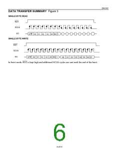
A clock cycle is a sequence of a falling edge followed by a rising edge. For data inputs, data must be
valid during the rising edge of the clock and data bits are output on the falling edge of clock. If the RST
input is low all data transfer terminates and the I/O pin goes to a high impedance state. Data transfer is
illustrated in Figure 3. At power–up, RST must be a logic 0 until VCC > 2.0 volts. Also SCLK must be at
a logic 0 when RST is driven to a logic 1 state.
DATA INPUT
Following the eight SCLK cycles that input a write command byte, a data byte is input on the rising edge
of the next eight SCLK cycles. Additional SCLK cycles are ignored should they inadvertently occur.
Data is input starting with bit 0.
DATA OUTPUT
Following the eight SCLK cycles that input a read command byte, a data byte is output on the falling
edge of the next eight SCLK cycles. Note that the first data bit to be transmitted occurs on the first falling
edge after the last bit of the command byte is written. Additional SCLK cycles retransmit the data bytes
should they inadvertently occur so long as RST remains high. This operation permits continuous burst
mode read capability. Also, the I/O pin is tri–stated upon each rising edge of SCLK. Data is output
starting with bit 0.
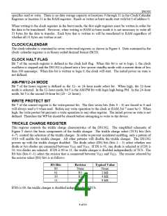
BURST MODE
Burst mode may be specified for either the clock/calendar or the RAM registers by addressing location 31
decimal (address/command bits 1 through 5 = logic 1). As before, bit 6 specifies clock or RAM and bit 0
3 of 14

 TGS [ Tiger Electronic Co.,Ltd ]