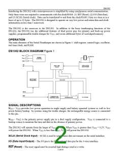
DS1302
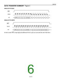
specifies read or write. There is no data storage capacity at locations 9 through 31 in the Clock/Calendar
Registers or location 31 in the RAM registers. Reads or writes in burst mode start with bit 0 of address 0.
When writing to the clock registers in the burst mode, the first eight registers must be written in order for
the data to be transferred. However, when writing to RAM in burst mode it is not necessary to write all
31 bytes for the data to transfer. Each byte that is written to will be transferred to RAM regardless of
whether all 31 bytes are written or not.
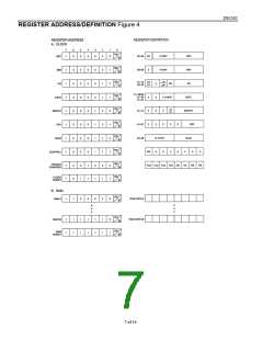
CLOCK/CALENDAR
The clock/calendar is contained in seven write/read registers as shown in Figure 4. Data contained in the
clock/ calendar registers is in binary coded decimal format (BCD).
CLOCK HALT FLAG
Bit 7 of the seconds register is defined as the clock halt flag. When this bit is set to logic 1, the clock
oscillator is stopped and the DS1302 is placed into a low–power standby mode with a current drain of less
than 100 nanoamps. When this bit is written to logic 0, the clock will start. The initial power on state is
not defined.
AM-PM/12-24 MODE
Bit 7 of the hours register is defined as the 12– or 24–hour mode select bit. When high, the 12–hour
mode is selected. In the 12–hour mode, bit 5 is the AM/PM bit with logic high being PM. In the 24–hour
mode, bit 5 is the second 10-hour bit (20 – 23 hours).
WRITE PROTECT BIT
Bit 7 of the control register is the write-protect bit. The first seven bits (bits 0 – 6) are forced to 0 and
will always read a 0 when read. Before any write operation to the clock or RAM, bit 7 must be 0. When
high, the write protect bit prevents a write operation to any other register. The initial power on state is not
defined. Therefore the WP bit should be cleared before attempting to write to the device.
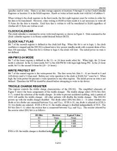
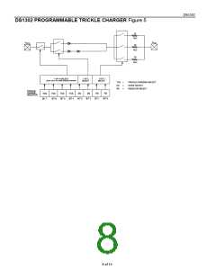
TRICKLE CHARGE REGISTER
This register controls the trickle charge characteristics of the DS1302. The simplified schematic of
Figure 5 shows the basic components of the trickle charger. The trickle charge select (TCS) bits (bits
4 -7) control the selection of the trickle charger. In order to prevent accidental enabling, only a pattern of
1010 will enable the trickle charger. All other patterns will disable the trickle charger. The DS1302
powers up with the trickle charger disabled. The diode select (DS) bits (bits 2 – 3) select whether one
diode or two diodes are connected between VCC2 and VCC1. If DS is 01, one diode is selected or if DS is
10, two diodes are selected. If DS is 00 or 11, the trickle charger is disabled independently of TCS. The
RS bits (bits 0 -1) select the resistor that is connected between VCC2 and VCC1. The resistor selected by
the resistor select (RS) bits is as follows:
RS Bits
00
Resistor
None
R1
Typical Value
None
01
2 kΩ
10
11
R2
4 kΩ
8 kΩ
R3
If RS is 00, the trickle charger is disabled independently of TCS.
4 of 14

 TGS [ Tiger Electronic Co.,Ltd ]