71M6521DE/71M6521FE
Energy Meter IC
DATASHEET
JANUARY 2008
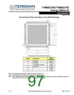
Recommended PCB Land Pattern for the QFN-68 Package
Recommended PCB Land Pattern Dimensions
Typical
Dimension
Symbol
Description
e
x
Lead pitch
0.4mm
Pad width
0.23mm
0.8mm
y
Pad length, see note 3
See note 1
d
A
G
6.3mm
6.63mm
7.2mm
Note 1: Do not place unmasked vias in region denoted by dimension “d”.
Note 2: Soldering of bottom internal pad is not required for proper operation.
Note 3: The ‘y’ dimension has been elongated to allow for hand soldering and reworking. Production assembly may allow this
dimension to be reduced as long as the ‘G’ dimension is maintained.
v1.0
© 2005-2008 TERIDIAN Semiconductor Corporation
Page: 97 of 101

 TERIDIAN [ TERIDIAN SEMICONDUCTOR CORPORATION ]