C2510Fx / CC2511Fx
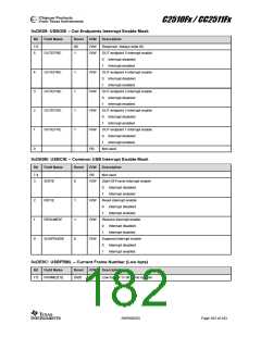
0xDE16: USBCNT0 – Number of Received Bytes in EP0 FIFO (USBINDEX=0)
Bit
Field Name
Reset
R/W
Description
7:6
5:0
-
R0
R
Not used
USBCNT0[5:0]
000000
Number of received bytes into EP 0 FIFO. Only valid when OUTPKT_RDY is
asserted
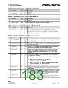
0xDE16: USBCNTL – Number of Bytes in EP{1 – 5} OUT FIFO Low
Bit
Field Name
Reset
R/W
Description
7:0
USBCNT[7:0]
0x00
R
8 LSB of number of received bytes into OUT FIFO selected by USBINDEX
register. Only valid when USBCSOL.OUTPKT_RDY is asserted.
0xDE17: USBCNTH – Number of Bytes in EP{1 – 5} OUT FIFO High
Bit
Field Name
Reset
R/W
Description
7:3
2:0
-
R0
R
Not used
USBCNT[10:8]
000
3 MSB of number of received bytes into OUT FIFO selected by USBINDEX
register. Only valid when USBCSOL.OUTPKT_RDY is set
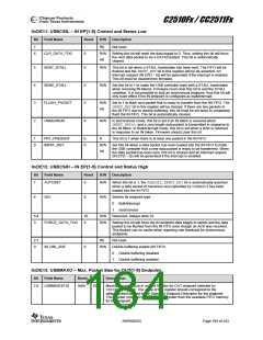
0xDE20: USBF0 – Endpoint 0 FIFO
Bit
Field Name
Reset
R/W
Description
7:0
USBF0[7:0]
0x00
R/W
Endpoint 0 FIFO. Reading this register unloads one byte from the EP0 FIFO.
Writing to this register loads one byte into the EP0 FIFO.
Note: The FIFO memory for EP0 is used for both incoming and outgoing data
packets.
0xDE22: USBF1 – Endpoint 1 FIFO
Bit
Field Name
Reset
R/W
Description
7:0
USBF1[7:0]
0x00
R/W
Endpoint 1 FIFO register. Reading this register unloads one byte from the EP1
OUT FIFO. Writing to this register loads one byte into the EP1 IN FIFO.
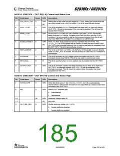
0xDE24: USBF2 – Endpoint 2 FIFO
Bit
Field Name
Reset
R/W
Description
7:0
USBF2[7:0]
0x00
R/W
See Endpoint 1 FIFO description.
0xDE26: USBF3 – Endpoint 3 FIFO
Bit
Field Name
Reset
R/W
Description
7:0
USBF3[7:0]
0x00
R/W
See Endpoint 1 FIFO description.
0xDE28: USBF4 – Endpoint 4 FIFO
Bit
Field Name
Reset
R/W
Description
7:0
USBF4[7:0]
0x00
R/W
See Endpoint 1 FIFO description.
0xDE2A: USBF5 – Endpoint 5 FIFO
Bit
Field Name
Reset
R/W
Description
7:0
USBF5[7:0]
0x00
R/W
See Endpoint 1 FIFO description.
SWRS055D
Page 186 of 243

 TAOS [ TEXAS ADVANCED OPTOELECTRONIC SOLUTIONS ]