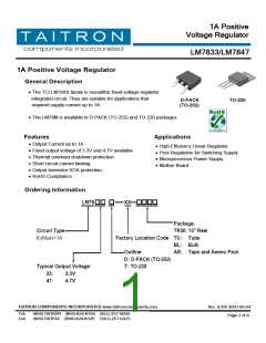
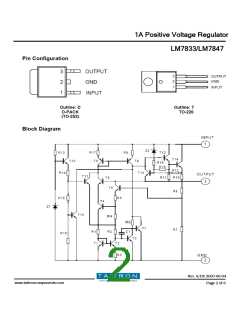
1A Positive Voltage Regulator
LM7833/LM7847
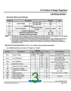
Absolute Maximum Ratings
Symbol
Description
Ratings
Unit
VOUT=3.3~18V
VOUT=20~24V
35
40
1
VIN
IOUT
PD
Input Voltage
V
A
Output Current
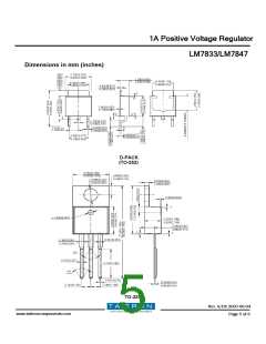
D-PACK (TO-252)
TO-220
Power Dissipation
Internally Limited
mW
TJ
Junction Temperature
150
TOPR
TSTG
Operating Temperature Range
Storage Temperature Range
-20 ~ 150
-55 ~ 150
° C
° C
Note: 1. Absolute maximum ratings are stress ratings only and functional device operation is not implied.
The device could be damaged beyond Absolute maximum ratings.
2. The maximum steady state usable output current are dependent on input voltage, heat sinking,
lead length of the package and copper pattern of PCB. The data are showed as electrical
characteristics table represents pulse test conditions with junction temperatures specified at
the initiation of test.
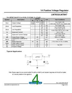
Electrical Characteristics (TJ=25° C, PD≦15W, unless otherwise specified)
For LM7833 (VIN=5.8V, IOUT=0.5A, C1=0.33µF, CO =0.1µF)
LM7833
Symbol
Description
Unit
Test Conditions
Min.
Typ.
Max.
3.168 3.30 3.432
V
IOUT=5mA-1.0A
5.8V≤VIN≤18.3V, IOUT=5mA-1.0A
IOUT=5mA-1.0A
VOUT
Output Voltage
3.135
-
-
3.465
33
V
-
-
-
-
-
-
-
-
mV
mV
mV
mV
mA
mA
mA
µV
∆VOUT
Load Regulation
-
17
IOUT=0.25A-0.75A
-
33
5.8V≤VIN≤18.3V
∆VOUT
IQ
Line Regulation
-
33
5.8V≤VIN≤18.3V, IOUT=1.0A
IOUT≦1.0A
Quiescent Current
-
8.0
1.0
0.5
-
-
5.8V≤VIN≤18.3V
∆IQ
Quiescent Current Change
-
IOUT=5mA-1.0A
eN
Output Noise Voltage
55
10Hz≤f≤100KHz
Temperature coefficient of
VOUT
∆VO/∆T
-
-0.4
-
mV/℃
IOUT=5mA
RR
IPEAK
ISC
Ripple Rejection
-
-
-
-
57
1.8
250
2.0
-
-
-
-
dB
A
6.3V≤VIN≤16.3V, f=120Hz
Peak Output Current
Short-Circuit Current
Dropout Voltage
-
mA
V
VIN=35V
-
VD
Rev. A/DX 2007-06-04
Page 3 of 6
www.taitroncomponents.com

 TAITRON [ TAITRON COMPONENTS INCORPORATED ]