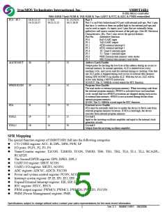
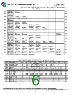
SyncMOS Technologies International, Inc.
SM89T16R1
8-Bits Micro-controller
With 64KB Flash ROM & 1KB RAM & Two UART & RTC & ADC & PWM embedded
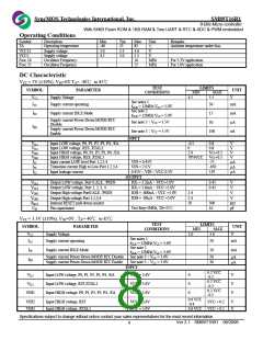
-0.4
VCC = 3.0V ~3.6V,
IIN1
ITL
ILI
Input current LOW level Port 1,2,3,4
Transition current High to Low Port 1,2,3,4
Input leakage current P0, /EA
-10
-75
-10
50
µA
µA
µA
VIN = 0.45V.
See note 4
400
10
VCC = 3.6V, VIN = 1.2 V
VCC = 3.0V ~3.6V,
0.45V<VIN<VCC
OUTPUT
I
OL = 7mA,VCC =3.3V
VOL1
VOL2
VOH1
VOH2
ISK1
ISK2
ISR1
ISR2
RRST
CIO
Output Low voltage, Port 0,ALE, /PSEN
Output Low voltage Port 1,2,3,4
Output High voltage Port0, ALE, /PSEN
0.4
0.4
V
V
V
IOL = 7mA,VCC =3.3V
IOH =-300uA,VCC =3.3V
2.4
2.4
Output High voltage Port 1,2,3,4
Sink Current Port 1, 2, 3, 4
Sink Current Port 0,ALE, /PSEN
Source Current Port 1, 2, 3, 4
Source Current Port 0,ALE, /PSEN
Internal RESET pull-down resistor
Pin capacitance
IOH =-20µA,VCC =3.3V
VCC = 3.3V, VIN = 0.4 V
VCC = 3.3V, VIN = 0.4 V
VCC = 3.3V, VIN = 2.4 V
VCC = 3.3V, VIN = 2.4 V
V
6
mA
mA
uA
mA
kΩ
pF
8
-80
-8
300
10
50
Test freq=1MHz, TA=25℃
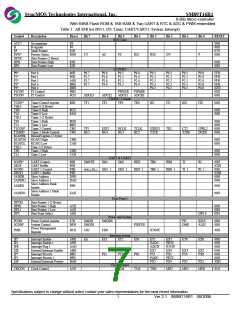
NOTES FOR DC ELECTRICAL CHARACTERISTICS
1.
2.
3.
4.
5.
The operating supply current is measured with all output disconnected;
XTAL1 driven with tr = tf = 5ns; VIL = VSS+0.5V; VIH=VCC-0.5V; XTAL2 not connect;/EA=RST=Port0=VCC
.
The IDLE MODE supply current is measured with all output pins disconnected; XTAL1 driven with tr = tf = 5ns; VIL = VSS+0.5V;
VIH=VCC-0.5V; XTAL2 not connect;/EA= Port0=VCC.
The POWER-DOWN MODE supply current is measured with all output pins disconnected; VIL = VSS+0.5V; VIH=VCC-0.5V; XTAL2 not
connect; /EA= Port0=VCC
.
Port 1, 2, 3, and 4 sources a transition current when they are being externally driven from HIGH to LOW. The transition current reaches
its maximum value when VIN is approximately 2V.
Capacities loading on port 0 and 2 may cause spurious noise to be superimposed on VOL of ALE and port 1, 3, and 4. The noise is due to
external bus capacitance discharging into port 0 and port 2 pins when these pins make 1-to-0 transitions during bus operations. In the
worst cases (capacities loading > 100pF), the noise pulse on the ALE pin may exceed 0.8V. In such cases, it may be desirable to qualify
ALE with a Schmitt Trigger, or use an address latch with a Schmitt trigger STROBE input.
Specifications subject to change without notice contact your sales representatives for the most recent information.
Ver 2.1 SM89T16R1 08/2006
9

 SYNCMOS [ SYNCMOS TECHNOLOGIES,INC ]