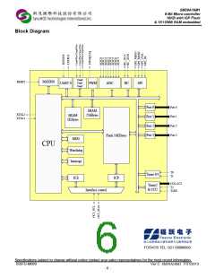
SM39A16M1
8-Bit Micro-controller
16KB with ISP Flash
& 1K+256B RAM embedded
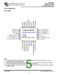
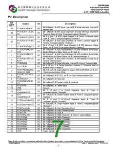
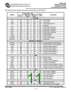
Pin Description
32L
Symbol
LQFP
I/O
I/O
I/O
I/O
I/O
I/O
I/O
I/O
Description
Bit 0 of port 1 & ADC input channel 0 & Serial interface channel 0
receive data
Bit 1 of port 1 & ADC input channel 1 & Serial interface channel 0
Transmit data & Timer 2 compare/capture Channel 0
Bit 2 of port 1 & ADC input channel 2 & Timer 2 external input
clock & Timer 2 compare/capture Channel 1
Bit 3 of port 1 & ADC input channel 3 & Timer 2 capture trigger &
Timer 2 compare/capture Channel 2
Bit 4 of port 1 & ADC input channel 4 & SPI interface Slave
Select pin & Timer 2 compare/capture Channel 3
Bit 5 of port 1 & ADC input channel 5 & SPI interface Serial Data
Master Output or Slave Input pin & Fault_B
Bit 6 of port 1 & ADC input channel 6 & SPI interface Serial Data
Master Input or Slave Output pin & External interrupt 0
Bit 7 of port 1 & ADC input channel 7 & SPI interface Clock pin &
Timer 0 external input
Bit 0 of port 3 & Serial interface channel 0 receive/Transmit data
Bit 1 of port 3 & Serial interface channel 0 Transmit data or
receive clock in mode 0
29
30
31
32
1
P1.0/ADC0/RXD0
P1.1/ADC1/TXD0/C
C0
P1.2/ADC2/T2/CC1
P1.3/ADC3/T2EX/C
C2
P1.4/ADC4/SS/CC3
P1.5/ADC5/MOSI/F
LTB
P1.6/ADC6/MISO/I
NT0
P1.7/ADC7/SPI_CL
K/T0
P3.0/RXD0
2
3
4
5
6
I/O
I/O
I/O
P3.1/TXD0
P3.2/TRIGADC/IIC_
SDA/OCI_SDA
P3.3/IIC_SCL/OCI_
SCL
P3.4/RESET
P3.5/XTAL2/CLKO
UT
Bit 2 of port 3 & external pin to trigger ADC & IIC SDA pin & On-
Chip Instrumentation SDA
7
I/O
8
9
I/O
I/O
I/O
I/O
Bit 3 of port 3 & IIC SCL pin & On-Chip Instrumentation SCL
Bit 4 of port 3 & Reset pin
10
Bit 5 of port 3 & Crystal output & clock out
11
12
P3.6/XTAL1
VSS
Bit 6 of port 3 & Crystal input
Ground
P2.0
/Cmp0NIn/CC0
P2.1
/Cmp0PIn/CC1
Bit
0 of port 2 & Cmp0 Negative Input & Timer 2
13
14
15
16
I/O
I/O
I/O
I/O
compare/capture Channel 0
Bit 1 of port 2 & Cmp0 Positive Input & Timer 2 compare/capture
Channel 1
Bit
2 of port 2 & Cmp1 Negative Input & Timer 2
P2.2/Cmp1NIn/CC2
P2.3/Cmp1PIn/CC3
compare/capture Channel 2
Bit 3 of port 2 & Cmp1 Positive Input & Timer 2 compare/capture
Channel 3
17
18
19
20
22
23
24
25
26
27
28
P2.4/Cmp2NIn
P2.5/Cmp2PIn
P2.6/FLTA
I/O
I/O
I/O
I/O
I/O
I/O
I/O
I/O
I/O
I/O
I
Bit 4 of port 2 & Cmp2 Negative Input
Bit 5 of port 2 & Cmp2 Positive Input
Bit 6 of port 2 & Fault_A
P0.7/PWM7/T1
P0.5/PWM5
P0.4/PWM4
P0.3/PWM3
P0.2/PWM2
P0.1/PWM1
P0.0/PWM0
VDD
Bit 7 of port 0 & PWM Channel 7 & Timer 1 external input
Bit 5 of port 0 & PWM Channel 5
Bit 4 of port 0 & PWM Channel 4
Bit 3 of port 0 & PWM Channel 3
Bit 2 of port 0 & PWM Channel 2
Bit 1 of port 0 & PWM Channel 1
Bit 0 of port 0 & PWM Channel 0
Power supply
Specifications subject to change without notice contact your sales representatives for the most recent information.
ISSFD-M069 Ver C SM39A16M1 7/31/2013
- 7 -

 SYNCMOS [ SYNCMOS TECHNOLOGIES,INC ]