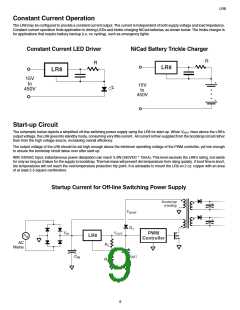
LR8
Ordering Information
Product marking for TO-243AA:
LR8❋
Package Options
TO-243AA*
LR8N8
TO-92
TO-252
where ❋ = 2-week alpha date code
LR8N3
LR8K4
*
Same as SOT-89. Product supplied on 2000 piece carrier tape reels.
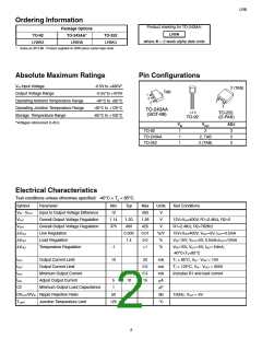
Absolute Maximum Ratings
Pin Configurations
VIN Input Voltage
-0.5V to +480V*
2 (TAB)
TAB
Output Voltage Range
-0.5V to +470V
-40°C to +85°C
-40°C to +125°C
-65°C to +150°C
1
2
Operating Ambient Temperature Range
Operating Junction Temperature Range
Storage Temperature Range
*Voltages referenced to ADJ.
1
3
3
TO-243AA
1 2 3
TO-252
(D-PAK)
(SOT-89)
TO-92
VIN
1
VOUT
ADJ
TO-92
2
3
3
3
TO-243AA
TO-252
1
2, TAB
2 (TAB)
1
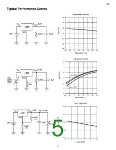
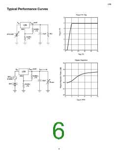
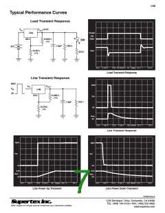
Electrical Characteristics
Test conditions unless otherwise specified: -40°C < TA < 85°C.
Symbol
VIN - VOUT
VOUT
Parameter
Min
12
Typ
Max
Units
Test Conditions
Input to Output Voltage Difference
Overall Output Voltage Regulation
Overall Output Voltage Regulation
Line Regulation
450
1.26
425
0.01
3.0
V
V
1.14
375
1.20
400
12V<VIN<400V, R1=2.4KΩ, R2=0
R1=2.4KΩ, R2=782KΩ
VOUT
V
∆VOUT
∆VOUT
∆VOUT
0.003
1.4
%/V
%
15V<VIN<400V, VOUT=5V, IOUT=0.5mA
VIN=15V, VOUT=5V, 0.5mA<IOUT<10mA
Load Regulation
Temperature Regulation
-1
+1
%
VIN=15V, VOUT=5V, IOUT=10mA,
-40°C<TA<85°C
IOUT
IOUT
IOUT
IADJ
C2
Output Current Limit
10
20
0.5
0.5
15
mA
mA
mA
µA
µF
TJ < 85°C, VIN - VOUT = 10V
TJ > 125°C, VIN - VOUT = 450V
Includes R1 and load current
Output Current Limit
Minimum Output Current
Adjust Output Current
0.3
10
5
1
Minimum Output Load Capacitance
DVOUT/DVIN Ripple Rejection Ratio
TLIMIT Junction Temperature Limit
50
125
60
dB
°C
120Hz, VOUT = 5V
2

 SUPERTEX [ Supertex, Inc ]