HV9901
Ordering Information
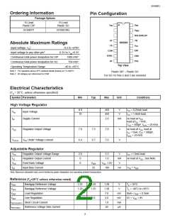
Pin Configuration
Package Options
16 Lead
Plastic DIP
16 Lead
Plastic SO
V
IN
V
V
DD
HV9901P
HV9901NG
REF
HOLD/DELAY
FB
GT
CS
HV9901
Absolute Maximum Ratings
V
CC
2
Input voltage, VIN
-0.5 to +470V
ENI
COM
SYNC
RT
Input voltage to any other pin 2
Continuous total power dissipation for DIP
Continuous total power dissipation for SO
Operating Temperature Range
-0.3V to VDD+0.3V
1000 mW 1
ENO
POL
750 mW 1
Top View
-40 to +85°C
Note 1: For operation above 25°C ambient derate linearly at 7.5 mW/°C.
Plastic DIP – Plastic SO
Note 2: All voltages are referenced to COM.
For SO-16 Pins 2 and 3 are removed
Electrical Characteristics
(TA = 25°C, unless otherwise specified)
Symbol Parameters
Min
Typ
Max
Unit
Conditions
High Voltage Regulator
8.0
10
450
450
V
V
ICC = 0.25mA load
ICC = 1.0mA load
VIN
IIN
Input Voltage
Supply Current
2.0
7.8
7.0
mA
no load at VDD,
load at ICC =1mA,
CGT = 500pF, fOSC = 25 KHz
VDD
Regulator Output Voltage
VDD Under Voltage Lockout
7.0
6.4
7.5
6.7
V
no load at VDD, load at
ICC =1mA, CGT = 500pF,
fOSC = 25 KHz
VUVLO
V
Adjustable Regulator
VCC
ICC
Regulator Output Voltage Range
2.0
0
5.5
1.0
V
mA
V
ICC =1.0mA load
Regulator Output Current
Feed Back Voltage
Input Bias Current
no load at VDD , See Note
VFB
IFB
0
VREF
25
VDD -1.0V
100
nA
VFB = VREF
Note: Maximum allowable load current limited by power dissipation and operating ambient temperature.
Reference (TA=25°C unless otherwise noted)
VREF
VREF
VREF
VREF
Bandgap Reference Voltage
Bandgap Reference Voltage
Load Regulation
1.22
1.20
1.25
1.25
1.28
1.30
7.0
5.0
1.0
20
V
TA = 25°C
V
TA = -40°C to +85°C
0mA < IREF < 0.3mA
6V < VDD < 8V
mV
mV
mA
µA
Line Regulation
2.0
IREF(SHORT) Short Circuit Current
IREF(SINK) Reference Voltage Sink Current
2

 SUPERTEX [ Supertex, Inc ]