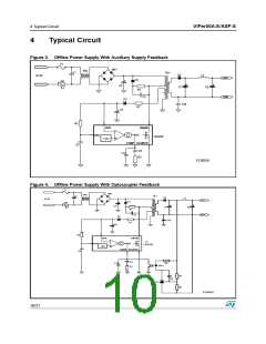
1 Electrical Data
VIPer50A-E/ASP-E
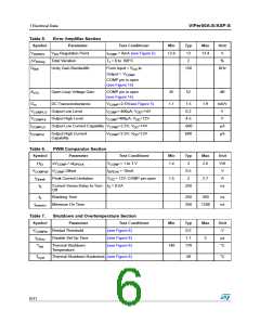
Table 5.
Symbol
Error Amplifier Section
Parameter
Test Conditions‘
Min
Typ
13
Max
Unit
V
V
V
Regulation Point
I = 0mA (see Figure 5)
COMP
12.6
13.4
DDREG
DD
∆V
Total Variation
T = 0 to 100°C
2
%
DDreg
J
G
Unity Gain Bandwidth
From Input = V to
150
KHz
BW
DD
Output = V
COMP
COMP pin is open
(see Figure 15)
A
Open Loop Voltage Gain
COMP pin is open
(see Figure 15)
45
52
dB
VOL
G
DC Transconductance
Output Low Level
V
=2.5V(see Figure 5)
COMP
1.1
1.5
0.2
1.9
mA/V
V
m
V
V
I
I
=-400µA; V =14V
DD
COMPLO
COMPHI
COMPLO
COMPHI
COMP
COMP
Output High Level
=400µA; V =12V
4.5
V
DD
I
I
Output Low Current Capability V
=2.5V; V =14V
-600
600
µA
µA
COMP
COMP
DD
Output High Current
Capability
V
=2.5V; V =12V
DD
Table 6.
Symbol
PWM Comparator Section
Parameter
Test Conditions‘
Min
Typ
2
Max
Unit
V/A
V
H
∆V
/ ∆I
V
= 1 to 3 V
1.4
2.6
ID
COMP
DPEAK
COMP
V
V
Offset
I
= 10mA
0.5
2
COMPoff
COMP
DPEAK
I
Peak Current Limitation
V
= 12V; COMP pin open
DD
1.5
2.7
A
Dpeak
t
Current Sense Delay to Turn- I = 0.5A
Off
250
ns
d
b
D
t
Blanking Time
250
350
360
ns
ns
t
Minimum On Time
1200
on(min)
Table 7.
Symbol
Shutdown and Overtemperature Section
Parameter
Restart Threshold
Disable Set Up Time
Test Conditions‘
Min
Typ
0.5
Max
Unit
V
V
(see Figure 8)
(see Figure 8)
(see Figure 8)
COMPth
t
1.7
5
µs
DISsu
T
Thermal Shutdown
Temperature
140
170
°C
tsd
T
Thermal Shutdown Hysteresis (see Figure 8)
40
°C
hyst
6/31

 STMICROELECTRONICS [ ST ]