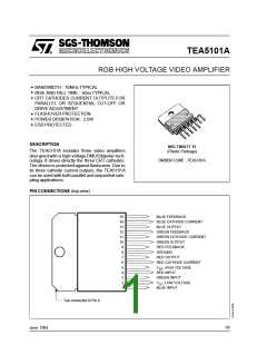
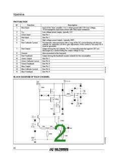
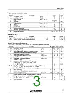
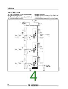
TEA5101A
ABSOLUTE MAXIMUM RATINGS
Symbol
Parameter
Value
250
35
Unit
V
VDD
VCC
Supply High Voltage
Supply Low Voltage
Pin 5
Pin 2
V
Output Current
to VDD
to Ground
Pins 7 - 10 - 13
IO
IO
Protected
8
mA
Output Current
to VDD
Pins 9 - 12 - 15
Pins 1 - 3 - 4
IF
IF
45
45
mA
mA
to Ground
Ij
Input Current
60
150
mA
°C
Tj
Junction Temperature
Operating Ambient Temperature
Storage Temperature
Toper
Tstg
0 to 70
°C
– 55 to + 150
°C
THERMAL DATA
Symbol
Parameter
Maximum Junction Case Thermal Resistance
Value
3
Unit
°C/W
°C/W
Rth(j-c)
Max.
Typ.
Rth(j-a) Typical Junction Ambient Thermal Resistance
35
ELECTRICAL CHARACTERISTICS
Tamb = 25oC ; VCC = 12V ; VDD = 200V ; AV = 50 (unless otherwise specified)
Symbol
VDD
Parameter
Min. Typ. Max.
Unit
V
High Supply Voltage
Low Supply Voltage
Pin 5
Pin 2
Pin 5
200
12
8
220
15
VCC
10
19
V
IDD
High Voltage Supply Internal DC Current (Vout 100V)
(without the current due to the feedback network )
12
mA
ICC
Low Voltage Supply DC Current
Pin 2
33
3
47
10
mA
V
Vsath
Output Saturation Voltage (High level)
Pins 7-10-13
IO = – 10 µA
RON
BW
Output Mos Transistor (Low level)
RON @ IO = 3 mA
Pins 7-10-13
1.7
kΩ
Bandwidth (– 3db) (measured on CRT cathodes)
(CLOAD : 10pF – R Protect = 1kΩ – Vout = 100V)
∆ Vout : 50 VPP
10
8
MHz
MHz
∆ Vout : 100 VPP
TR - TF Rise Time and Fall Time : measured between 10% and 90% of output
pulse (CLOAD : 10 pF – R Protect = 1 kΩ – Vout = 100 V)
∆ Vout : 100 VPP
50
ns
GO
P
Open Loop Gain
47
50
3.5
3.8
dB
W
Internal Power Dissipation (see calculation below)
Internal Voltage Reference
VREF
Pins 1-3-4
Pins 1-3-4
3.55
4.05
5
V
Internal Reference Voltage Difference Between 2 Channels
Voltage Reference Temperature Coefficient
Input Bias Current (Vout : 100 V)
Input Resistance
%
– 5
15
14
mV/°C
µA
IIB
RI
kΩ
3/6

 STMICROELECTRONICS [ ST ]