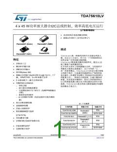
TDA75610LV
List of figures
List of figures
Figure 1.
Figure 2.
Figure 3.
Figure 4.
Figure 5.
Figure 6.
Figure 7.
Figure 8.
Figure 9.
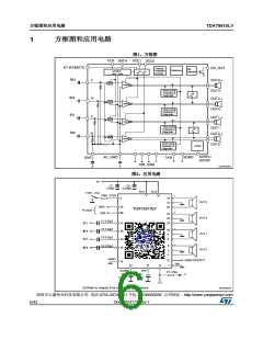
Block diagram. . . . . . . . . . . . . . . . . . . . . . . . . . . . . . . . . . . . . . . . . . . . . . . . . . . . . . . . . . . . 6
Application circuit . . . . . . . . . . . . . . . . . . . . . . . . . . . . . . . . . . . . . . . . . . . . . . . . . . . . . . . . . 6
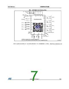
Application circuit (TDA75610LVPD) . . . . . . . . . . . . . . . . . . . . . . . . . . . . . . . . . . . . . . . . . . 7
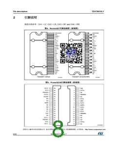
Pin connection diagram of the Flexiwatt27 (top of view). . . . . . . . . . . . . . . . . . . . . . . . . . . . 8
Pin connection diagram of the PowerSO36 slug up (top of view). . . . . . . . . . . . . . . . . . . . . 8
Quiescent current vs. supply voltage . . . . . . . . . . . . . . . . . . . . . . . . . . . . . . . . . . . . . . . . . 15
Output power vs. supply voltage (4 Ω) . . . . . . . . . . . . . . . . . . . . . . . . . . . . . . . . . . . . . . . . 15
Output power vs. supply voltage (2 Ω) . . . . . . . . . . . . . . . . . . . . . . . . . . . . . . . . . . . . . . . . 15
Distortion vs. output power (4 Ω, STD). . . . . . . . . . . . . . . . . . . . . . . . . . . . . . . . . . . . . . . . 15
Figure 10. Distortion vs. output power (4 Ω, HI-EFF). . . . . . . . . . . . . . . . . . . . . . . . . . . . . . . . . . . . . . 15
Figure 11. Distortion vs. output power (2 Ω, STD). . . . . . . . . . . . . . . . . . . . . . . . . . . . . . . . . . . . . . . . 15
Figure 12. Distortion vs. output power (2 Ω, HI-EFF). . . . . . . . . . . . . . . . . . . . . . . . . . . . . . . . . . . . . . 16
Figure 13. Distortion vs. output power V = 6 V (4 Ω, STD). . . . . . . . . . . . . . . . . . . . . . . . . . . . . . . . . 16
s
Figure 14. Distortion vs. frequency (4 Ω) . . . . . . . . . . . . . . . . . . . . . . . . . . . . . . . . . . . . . . . . . . . . . . . 16
Figure 15. Distortion vs. frequency (2 Ω) . . . . . . . . . . . . . . . . . . . . . . . . . . . . . . . . . . . . . . . . . . . . . . . 16
Figure 16. Crosstalk vs. frequency. . . . . . . . . . . . . . . . . . . . . . . . . . . . . . . . . . . . . . . . . . . . . . . . . . . . 16
Figure 17. Supply voltage rejection vs. frequency . . . . . . . . . . . . . . . . . . . . . . . . . . . . . . . . . . . . . . . . 16
Figure 18. Power dissipation vs. average output power (audio program simulation, 4 Ω). . . . . . . . . . 17
Figure 19. Power dissipation vs. average output power (audio program simulation, 2 Ω). . . . . . . . . . 17
Figure 20. Total power dissipation and efficiency vs. output power (4 Ω, HI-EFF, Sine). . . . . . . . . . . 17
Figure 21. Total power dissipation and efficiency vs. output power (4 Ω, STD, Sine) . . . . . . . . . . . . . 17
Figure 22. ITU R-ARM frequency response, weighting filter for transient pop. . . . . . . . . . . . . . . . . . . 17
Figure 23. Turn-on diagnostic: working principle . . . . . . . . . . . . . . . . . . . . . . . . . . . . . . . . . . . . . . . . . 18
Figure 24. SVR and output behavior (Case 1: without turn-on diagnostic) . . . . . . . . . . . . . . . . . . . . . 18
Figure 25. SVR and output pin behavior (Case 2: with turn-on diagnostic) . . . . . . . . . . . . . . . . . . . . . 19
Figure 26. Short circuit detection thresholds . . . . . . . . . . . . . . . . . . . . . . . . . . . . . . . . . . . . . . . . . . . . 19
Figure 27. Load detection thresholds - high gain setting . . . . . . . . . . . . . . . . . . . . . . . . . . . . . . . . . . . 19
Figure 28. Load detection threshold - low gain setting. . . . . . . . . . . . . . . . . . . . . . . . . . . . . . . . . . . . . 19
Figure 29. Restart timing without diagnostic enable (permanent) - Each 1 mS time,
a sampling of the fault is done . . . . . . . . . . . . . . . . . . . . . . . . . . . . . . . . . . . . . . . . . . . . . . 20
Figure 30. Restart timing with diagnostic enable (permanent). . . . . . . . . . . . . . . . . . . . . . . . . . . . . . . 20
Figure 31. Current detection high: load impedance |Z| vs. output peak voltage . . . . . . . . . . . . . . . . . 22
Figure 32. Current detection low: load impedance |Z| vs. output peak voltage . . . . . . . . . . . . . . . . . . 22
Figure 33. Thermal foldback diagram . . . . . . . . . . . . . . . . . . . . . . . . . . . . . . . . . . . . . . . . . . . . . . . . . 24
Figure 34. Worst case battery cranking curve sample 1 . . . . . . . . . . . . . . . . . . . . . . . . . . . . . . . . . . . 25
Figure 35. Worst case battery cranking curve sample 2 . . . . . . . . . . . . . . . . . . . . . . . . . . . . . . . . . . . 25
Figure 36. Upwards fast battery transitions diagram . . . . . . . . . . . . . . . . . . . . . . . . . . . . . . . . . . . . . . 26
Figure 37. Inputs impedance matching circuit . . . . . . . . . . . . . . . . . . . . . . . . . . . . . . . . . . . . . . . . . . . 27
Figure 38. High efficiency - basic structure . . . . . . . . . . . . . . . . . . . . . . . . . . . . . . . . . . . . . . . . . . . . . 28
2
Figure 39. Data validity on the I C bus . . . . . . . . . . . . . . . . . . . . . . . . . . . . . . . . . . . . . . . . . . . . . . . . 30
2
Figure 40. Timing diagram on the I C bus . . . . . . . . . . . . . . . . . . . . . . . . . . . . . . . . . . . . . . . . . . . . . . 30
2
Figure 41. Acknowledge on the I C bus. . . . . . . . . . . . . . . . . . . . . . . . . . . . . . . . . . . . . . . . . . . . . . . . 30
Figure 42. Flexiwatt27 (horizontal) mechanical data and package dimensions. . . . . . . . . . . . . . . . . . 37
Figure 43. Flexiwatt27 (vertical) mechanical data and package dimensions. . . . . . . . . . . . . . . . . . . . 38
Figure 44. Flexiwatt27 (SMD) mechanical data and package dimensions . . . . . . . . . . . . . . . . . . . . . 39
Figure 45. PowerSO36 (slug up) mechanical data and package dimensions . . . . . . . . . . . . . . . . . . . 40
DocID024173 Rev 7
5/42
5

 STMICROELECTRONICS [ ST ]