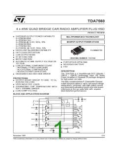
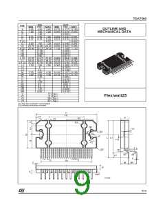
TDA7560
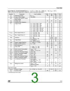
ELECTRICAL CHARACTERISTICS (VS = 13.2V; f = 1KHz; Rg = 600Ω; RL = 4Ω; Tamb = 25°C;
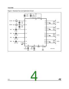
Refer to the test and application diagram, unless otherwise specified.)
Symbol
Iq1
Parameter
Quiescent Current
Test Condition
Min.
Typ.
Max.
320
Unit
mA
mV
mV
R =
120
200
∞
L
VOS
Output Offset Voltage
Play Mode
80
±
±
dVOS
During mute ON/OFF output
offset voltage
80
Gv
dGv
Po
Voltage Gain
25
26
27
dB
dB
Channel Gain Unbalance
Output Power
±1
VS = 13.2V; THD = 10%
VS = 13.2V; THD = 1%
VS = 14.4V; THD = 10%
VS = 14.4V; THD = 1%
23
16
28
20
25
19
30
23
W
W
W
W
VS = 13.2V; THD = 10%, 2Ω
42
32
50
40
45
34
55
43
W
W
W
W
V = 13.2V; THD = 1%, 2
Ω
S
VS = 14.4V; THD = 10%, 2Ω
VS = 14.4V; THD = 1%, 2Ω
Po EIAJ
Po max.
THD
EIAJ Output Power (*)
Max. Output Power (*)
Distortion
VS = 13.7V; RL = 4Ω
41
75
45
77
W
W
V = 13.7V; R = 2
Ω
S
L
V = 14.4V; R = 4
50
80
W
W
Ω
S
L
VS = 14.4V; RL = 2Ω
Po = 4W
0.006
0.015
0.05
0.07
%
%
P = 10W; R = 2
Ω
o
L
eNo
Output Noise
”A” Weighted
35
50
50
70
V
µ
µV
Bw = 20Hz to 20KHz
f = 100Hz; Vr = 1Vrms
PO = 0.5W
SVR
fch
Supply Voltage Rejection
High Cut-Off Frequency
Input Impedance
50
100
80
70
dB
300
100
KHz
KΩ
Ri
120
CT
Cross Talk
f = 1KHz PO = 4W
f = 10KHz PO = 4W
60
70
60
–
–
dB
dB
ISB
Ipin4
St-By Current Consumption
St-by pin Current
VSt-By = 1.5V
VSt-By = 1.5V to 3.5V
(Amp: ON)
75
A
µ
±10
µA
V
VSB out
VSB in
AM
St-By Out Threshold Voltage
St-By in Threshold Voltage
Mute Attenuation
3.5
(Amp: OFF)
POref = 4W
1.5
1.5
V
80
90
7
dB
V
VM out
VM in
VAM in
Mute Out Threshold Voltage
Mute In Threshold Voltage
VS Automute Threshold
(Amp: Play)
3.5
(Amp: Mute)
(Amp: Mute)
V
Att 80dB; POref = 4W
6.5
V
V
≥
(Amp: Play)
Att < 0.1dB; PO = 0.5W
7.5
12
8
Ipin22
Muting Pin Current
VMUTE = 1.5V
(Sourced Current)
7
18
A
µ
V
MUTE = 3.5V
-5
18
µA
HSD SECTION
Vdropout
Dropout Voltage
IO = 0.35A; VS = 9 to 16V
0.25
0.6
V
Iprot
Current Limits
400
800
mA
(*) Saturated square wave output.
3/10

 STMICROELECTRONICS [ ST ]