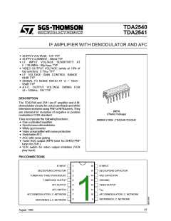
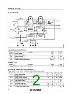
TDA2540 - TDA2541
ELECTRICAL OPERATING CHARACTERISTICS (continued)
Tamb = 25 °C; V (11 – 13) = 12 V; f = 38.9 MHz (unless otherwise specified)
Symbol
S/N
Parameter
Signal to Noise Ratio (VI = 10mV) (see note 1)
Bandwidth of Video Amplifier (– 3dB)
Min.
Typ.
58
6
Max.
Unit
dB
50
B
MHz
%
dG
Differential Gain
4
10
10
30
30
dφ
Differential Phase
2
%
V12-13
V12-13
Carrier Signal at Video Output (VI = 10mV)
2nd Harmonic of Carrier at Video Output (VI = 10mV)
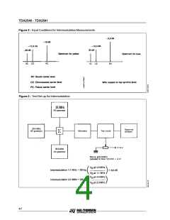
Intermodulation at 1.1MHz (blue) (see Figures 2 and 3)
Intermodulation at 1.1MHz (yellow) (see Figures 2 and 3)
Intermodulation at 3.3MHz (blue) (see Figures 2 and 3)
VCR Switches Off Output at : (VCR = low Level)
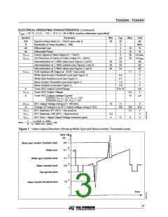
White Spot Inverter Threshold Level (see Figure 1)
White Spot Insertion Level (see Figure 1)
Noise Inverter Threshold Level (see Figure 1)
Noise Insertion Level (see Figure 1)
4
mVRMS
mVRMS
dB
20
60
50
54
46
46
46
dB
dB
V14-13
1.1
V
6.6
4.7
V
V
1.8
V
3.8
V
I4
V14-13
I4
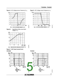
Tuner AGC output Current Range
0 to 10
mA
V
Tuner AGC Output Voltage
0.3
15
Tuner AGC Output Leakage Current
TDA2541 V14-13 = 11V, V4-13 = 12V
TDA2540 V14-13 = 5V, V4-13 = 12V
µA
∆V5-13
∆f
AFC Output Voltage Swing (∆f = 100 kHz)
10
11
V
kHz
V
Change of Frequency at AFC Output (voltage swing of 10V)
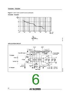
AFC Switches OFF (AFC = low level) at :
100
200
2.5
V6-13
V6-13
V5-13
AFC Switches LOW (AFC = High level) at :
AFC Zero = Signal Output Voltage (minimum gain)
3.2
4
V
6
8
V
V
O (black to white)
S
N
Note : 1.
=
(dB)
VN (RMS at B = 5MHz)
Figure 1 : Video Output Waveform Showing White Spot and Noise Inverter Threshold Levels
3/7

 STMICROELECTRONICS [ ST ]