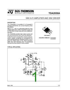
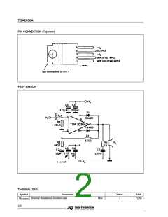
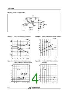
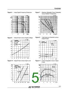
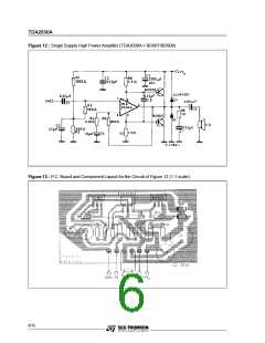
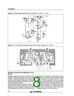
TDA2030A
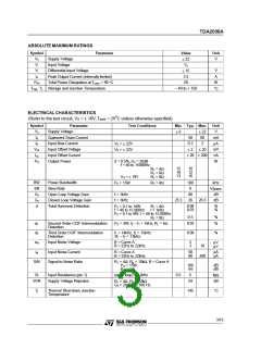
ABSOLUTE MAXIMUM RATINGS
Symbol
Parameter
Value
Unit
Vs
Vi
Supply Voltage
V
± 22
Input Voltage
Vs
± 15
Vi
Differential Input Voltage
V
A
Io
Peak Output Current (internally limited)
Total Power Dissipation at Tcase = 90 °C
Storage and Junction Temperature
3.5
Ptot
Tstg, Tj
20
W
– 40 to + 150
°
C
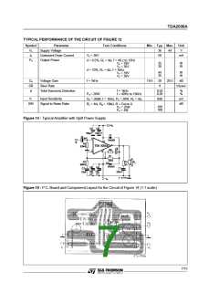
ELECTRICAL CHARACTERISTICS
(Refer to the test circuit, VS = ± 16V, Tamb = 25oC unless otherwise specified)
Symbol
Parameter
Supply Voltage
Test Conditions
Min. Typ. Max.
Unit
V
Vs
Id
± 6
± 22
80
2
Quiescent Drain Current
Input Bias Current
Input Offset Voltage
Input Offset Current
Output Power
50
mA
µA
mV
nA
W
Ib
0.2
VS = ± 22V
Vos
Ios
PO
VS = ± 22V
± 2
± 20
±
20 ± 200
d = 0.5%, Gv = 26dB
f = 40 to 15000Hz
15
10
13
18
12
16
RL = 4Ω
RL = 8Ω
RL = 8Ω
V
S = ± 19V
BW
SR
Gv
Gv
d
Power Bandwidth
Po = 15W
RL = 4Ω
100
8
kHz
V/µsec
dB
Slew Rate
Open Loop Voltage Gain
Closed Loop Voltage Gain
Total Harmonic Distortion
f = 1kHz
f = 1kHz
80
26
25.5
26.5
dB
0.08
0.03
%
%
Po = 0.1 to 14W
f = 40 to 15 000Hz
RL = 4Ω
f = 1kHz
Po = 0.1 to 9W, f = 40 to 15 000Hz
0.5
%
%
RL = 8Ω
d2
d3
eN
Second Order CCIF Intermodulation
Distortion
PO = 4W, f2 – f1 = 1kHz, RL = 4Ω
0.03
Third Order CCIF Intermodulation
Distortion
f1 = 14kHz, f2 = 15kHz
2f1 – f2 = 13kHz
0.08
%
Input Noise Voltage
Input Noise Current
Signal to Noise Ratio
B = Curve A
B = 22Hz to 22kHz
2
3
µV
µV
10
iN
B = Curve A
B = 22Hz to 22kHz
50
80
pA
pA
200
S/N
RL = 4Ω, Rg = 10kΩ, B = Curve A
106
94
dB
dB
PO = 15W
PO = 1W
Ri
Input Resistance (pin 1)
Supply Voltage Rejection
(open loop) f = 1kHz
0.5
5
MΩ
SVR
54
dB
RL = 4Ω, Rg = 22kΩ
Gv = 26dB, f = 100 Hz
Tj
Thermal Shut-down Junction
Temperature
145
°C
3/15

 STMICROELECTRONICS [ ST ]