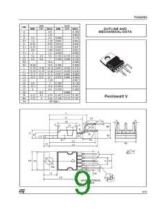
TDA2003
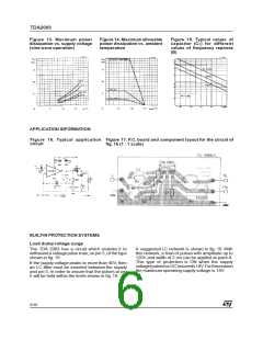
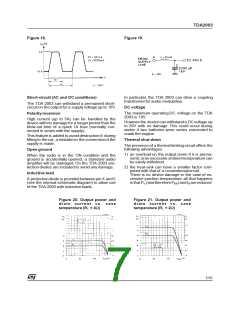
PRATICAL CONSIDERATION
Printed circuit board
The layout shown in fig. 17 is recommended. If
different layouts are used, the ground points of
input 1 and input 2 must be well decoupled from
thegroundoftheoutputthroughwhicha ratherhigh
current flows.
packageand the heat-sink.Pinlength shouldbe as
short as possible.The soldering temperature must
not exceed 260 C for 12 seconds.
°
Application suggestions
The recommended component values are those
shown in the applicationcircuits of fig.16.
Different valuescan be used.The followingtableis
intended to aid the car-radio designer.
Assembly suggestion
No electrical insulation is required between the
Recommmended
Larger than
Smaller than
Component
Purpose
Input DC
value
recommended value recommended value C1
Noise at switch-on,
switch-off
C1
2.2 µF
decoupling
C2
C3
C4
Ripple rejection
Supply bypassing
Output coupling to load
Degradation of SVR
Danger of oscillation
470
0.1
F
µ
F
µ
1000
F
Higher low frequency
cutoff
µ
C5
CX
Frequency stability
Danger of oscillation at
high frequencies with
inductive loads
0.1 µF
1
Upper frequency cutoff
Setting of gain
Lower bandwidth
Larger bandwidth
2
B R1
π
R1
R2
Increase of drain current
(Gv-1) • R2
2.2
Setting of gain
and SVR
Degradation of SVR
Ω
R3
RX
1
Ω
Frequency stability
Danger of oscillation at
high frequencies with
inductive loads
Upper frequency cutoff
Poor high frequency
attenuation
Danger of oscillation
20 R2
8/10

 STMICROELECTRONICS [ ST ]