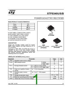
STPS340U/S/B
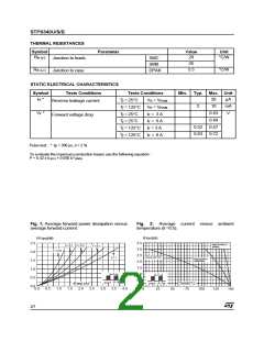
Fig. 5: Reverse leakage current versus reverse
voltage applied (Typical values).
Fig. 6: Junction capacitance versus reverse
voltage applied (Typical values).
IR(A)
C(pF)
1E-2
500
Tj=150°C
F=1MHz
Tj=25°C
200
Tj=125°C
1E-3
100
50
Tj=100°C
1E-4
Tj=75°C
20
VR(V)
VR(V)
1E-5
10
1
2
5
10
20
50
0
5
10
15
20
25
30
35
40
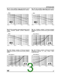
Fig. 7: Forward voltage drop versus forward
current (Maximum values).
Fig. 8-1: Thermal resistance junction to ambient
versus copper surface under each lead (Epoxy printed
circuit board FR4, copper thickness: 35µm) (SMB).
Rth(j-a) (°C/W)
IFM(A)
10.00
120
Typical values
Tj=150°C
100
80
1.00
Tj=125°C
60
0.10
40
20
VFM(V)
S(Cu) (cm²)
0.01
0
0.0 0.1 0.2 0.3 0.4 0.5 0.6 0.7 0.8 0.9 1.0
0
1
2
3
4
5
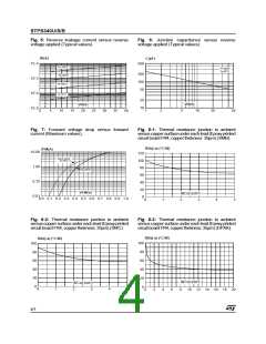
Fig. 8-2: Thermal resistance junction to ambient
versus copper surface under each lead (Epoxy printed
circuit board FR4, copper thickness: 35µm) (SMC).
Fig. 8-3: Thermal resistance junction to ambient
versus copper surface under each lead (Epoxy printed
circuit board FR4, copper thickness: 35µm) (DPAK).
Rth(j-a) (°C/W)
Rth(j-a) (°C/W)
100
100
80
60
40
80
60
40
20
20
S(Cu) (cm²)
S(Cu) (cm²)
0
0
0
1
2
3
4
5
0
2
4
6
8
10 12 14 16 18 20
4/7

 STMICROELECTRONICS [ ST ]