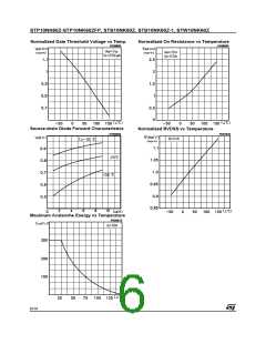
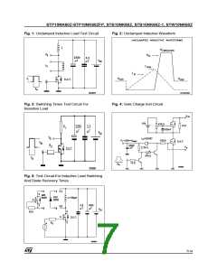
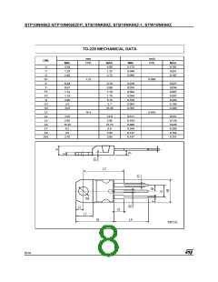
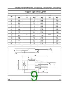
STP10NK60Z-STP10NK60ZFP, STB10NK60Z, STB10NK60Z-1, STW10NK60Z
ABSOLUTE MAXIMUM RATINGS
Symbol
Parameter
Value
TO-220FP
Unit
TO-220/
TO-247
2
2
D PAK/I PAK
V
Drain-source Voltage (V = 0)
600
600
± 30
V
V
DS
GS
V
Drain-gate Voltage (R = 20 kΩ)
DGR
GS
V
Gate- source Voltage
V
GS
I
Drain Current (continuous) at T = 25°C
10
5.7
36
10 (*)
10
5.7
36
A
D
D
C
I
Drain Current (continuous) at T = 100°C
5.7 (*)
36 (*)
35
A
C
I
( )
Drain Current (pulsed)
A
DM
P
Total Dissipation at T = 25°C
115
0.92
156
1.25
W
W/°C
V
TOT
C
Derating Factor
0.28
V
Gate source ESD
4000
ESD(G-S)
(HBM-C=100pF, R=1.5KΩ)
dv/dt (1)
Peak Diode Recovery voltage slope
Insulation Withstand Voltage (DC)
4.5
2500
V/ns
V
V
-
-
ISO
T
T
stg
Operating Junction Temperature
Storage Temperature
j
-55 to 150
°C
( ) Pulse width limited by safe operating area
(1) I ≤10A, di/dt ≤200A/µs, V ≤ V
, T ≤ T
j JMAX.
SD
DD
(BR)DSS
(*) Limited only by maximum temperature allowed
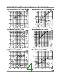
THERMAL DATA
TO-220
2
TO-220FP
TO-247
Unit
D PAK
2
I PAK
Rthj-case
Rthj-pcb
Thermal Resistance Junction-case Max
1.09
3.6
0.8
°C/W
°C/W
Thermal Resistance Junction-pcb Max
(When mounted on minimum Footprint)
60
Rthj-amb
Thermal Resistance Junction-ambient
Max
62.5
50
°C/W
°C
T
Maximum Lead Temperature For
Soldering Purpose
300
l
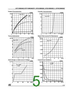
AVALANCHE CHARACTERISTICS
Symbol
Parameter
Max Value
Unit
I
AR
Avalanche Current, Repetitive or Not-Repetitive
9
A
(pulse width limited by T max)
j
E
E
Single Pulse Avalanche Energy
300
3.5
mJ
mJ
AS
(starting T = 25 °C, I = I , V = 50 V)
j
D
AR
DD
Repetitive Avalanche Energy
(Pulse with limited by T max.)
AR
j
GATE-SOURCE ZENER DIODE
Symbol
BV
Parameter
Test Conditions
Min.
Typ.
Max.
Unit
Gate-Source Breakdown
Voltage
Igs=± 1mA (Open Drain)
30
V
GSO
PROTECTION FEATURES OF GATE-TO-SOURCE ZENER DIODES
The built-in back-to-back Zener diodes have specifically been designed to enhance not only the device’s
ESD capability, but also to make them safely absorb possible voltage transients that may occasionally be
applied from gate to source. In this respect the Zener voltage is appropriate to achieve an efficient and
cost-effective intervention to protect the device’s integrity. These integrated Zener diodes thus avoid
the usage of external components.
2/14

 STMICROELECTRONICS [ ST ]