STM32F302xx/STM32F303xx
Pinouts and pin description
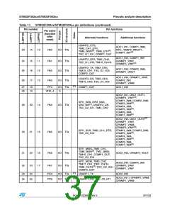
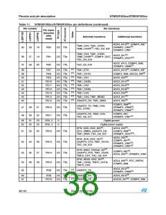
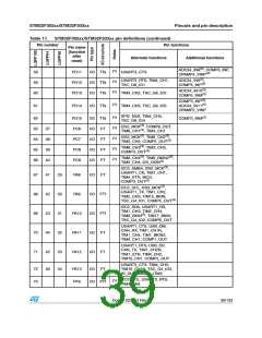
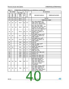
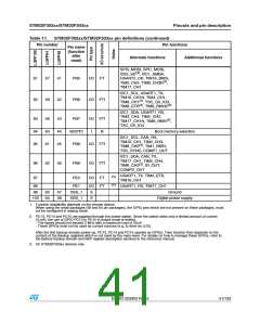
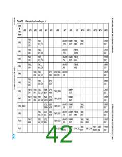
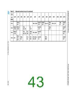
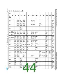
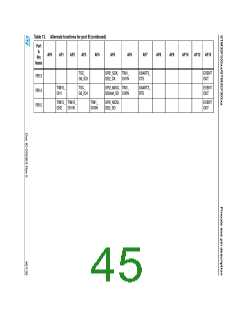
Table 11. STM32F302xx/STM32F303xx pin definitions (continued)
Pin number
Pin functions
Pin name
(function
after
Alternate functions
Additional functions
reset)
SPI3_MOSI, SPI1_MOSI,
I2S3_SD(3), I2C1_SMBA,
USART2_CK, TIM16_BKIN,
91
57
58
41
PB5
PB6
I/O FT
TIM3_CH2, TIM8_CH3N(3)
TIM17_CH1
,
I2C1_SCL, USART1_TX,
TIM16_CH1N, TIM4_CH1,
92
42
I/O FTf
I/O FTf
TIM8_CH1(3), TSC_G5_IO3,
TIM8_ETR(3), TIM8_BKIN2(3)
I2C1_SDA, USART1_RX,
TIM3_CH4, TIM4_CH2,
93
94
95
59
60
61
43
44
45
PB7
BOOT0
PB8
TIM17_CH1N, TIM8_BKIN(3)
TSC_G5_IO4
,
I
B
Boot memory selection
I2C1_SCL, CAN_RX,
TIM16_CH1, TIM4_CH3,
TIM8_CH2(3), TIM1_BKIN,
TSC_SYNC, COMP1_OUT
I/O FTf
I2C1_SDA, CAN_TX,
TIM17_CH1, TIM4_CH4,
TIM8_CH3(3), IR_OUT,
COMP2_OUT
96
97
62
46
PB9
PE0
I/O FTf
I/O FT
USART1_TX, TIM4_ETR,
TIM16_CH1
(1)
(1)
98
99
PE1
I/O FT
USART1_RX, TIM17_CH1
63
64
47
48
VSS_1
VDD_1
S
S
Ground
Digital power supply
100
1. Function availability depends on the chosen device.
When using the small packages (48 and 64 pin packages), the GPIO pins which are not present on these packages, must
not be configured in analog mode.
2. PC13, PC14 and PC15 are supplied through the power switch. Since the switch sinks only a limited amount of current
(3 mA), the use of GPIO PC13 to PC15 in output mode is limited:
- The speed should not exceed 2 MHz with a maximum load of 30 pF
- These GPIOs must not be used as current sources (e.g. to drive an LED).
After the first backup domain power-up, PC13, PC14 and PC15 operate as GPIOs. Their function then depends on the
content of the Backup registers which is not reset by the main reset. For details on how to manage these GPIOs, refer to
the Battery backup domain and BKP register description sections in the reference manual.
3. On STM32F303xx devices only.
Doc ID 023353 Rev 5
41/133

 STMICROELECTRONICS [ ST ]