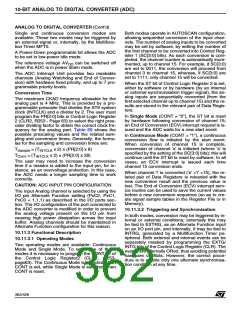
10-BIT ANALOG TO DIGITAL CONVERTER (ADC)
ANALOG TO DIGITAL CONVERTER (Cont’d)
The effect of either of these synchronisation
modes is to set the ST bit by hardware. This bit is
reset, in Single Mode only, at the end of each
group of conversions. In Continuous Mode, all trig-
ger pulses after the first are ignored.
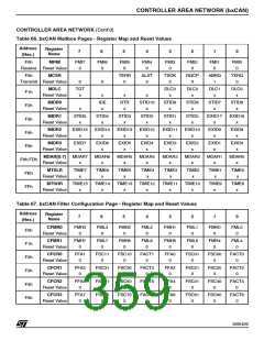
rupt. The four threshold voltages are user pro-
grammable in dedicated registers pairs (R244 to
R251, page 63). Only the 4 MSBs of the Compare
Results Register are used as flags, each of the
four MSBs being associated with a threshold con-
dition.
The synchronisation sources must be at a logic
low level for at least the duration of two INTCLK
cycles and, in Single Mode, the period between
trigger pulses must be greater than the total time
required for a group of conversions. If a trigger oc-
curs when the ST bit is still set, i.e. when a conver-
sion is still in progress, it will be ignored.
Following a reset, these flags are reset. During
normal ADC operation, the CRR bits are set, in or-
der to flag an out of range condition and are auto-
matically reset by hardware after a software reset
of the Analog Watchdog Request flag in the ICR
Register.
Note: The external trigger will set the CLR2.ST bit
10.11.3.4 Power Down Mode
even if the CLR2.POW is reset.
Before enabling an ADC conversion, the POW bit
of the Control Logic Register must be set; this
must be done at least 10 µs before the first conver-
sion start, in order to correctly bias the analog sec-
tion of the converter circuitry.
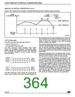
10.11.3.3 Analog Watchdog
Two internal Analog Watchdogs are available for
highly flexible automatic threshold monitoring of
external analog signal levels. Depending on the
value of the CC[3:0] bits in Control Logic Register1
these two watchdog are mapped onto 2 of the 16
available adjacent channels, allowing the user to
set the channel to be monitored. Refer to Table 68
to see the possible choices for this feature.
When the ADC is not required, the POW bit may
be reset in order to reduce the total power con-
sumption. This is the reset configuration, and this
state is also selected automatically when the ST9
is placed in Halt Mode (following the execution of
the haltinstruction).
Analog watchdog channels (named as A and B)
monitor an acceptable voltage level window for the
converted analog inputs. The external voltages
applied to inputs A and B are considered normal
while they remain below their respective Upper
thresholds, and above or at their respective Lower
thresholds.
Figure 156. Analog Watchdog Function
Analog Voltage
Upper Threshold
Normal Area
When the external signal voltage level is greater
than, or equal to, the upper programmed voltage
limit, or when it is less than the lower programmed
voltage limit, a maskable interrupt request is gen-
erated and the Compare Results Register is up-
dated in order to flag the threshold (Upper or Low-
er) and channel (A or B) responsible for the inter-
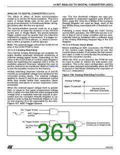
Figure 157. ADC Trigger Source
(Window Guarded)
Lower Threshold
Ext. Trigger Enable
ADC Trigger
EXTRG
Int. Trigger Enable
Start group of conversions
Continuous or Single mode
On-Chip Event
MFT0
Software Trigger
363/426
9

 STMICROELECTRONICS [ ST ]