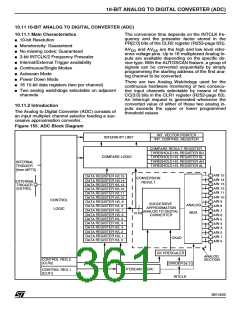
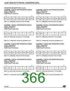
10-BIT ANALOG TO DIGITAL CONVERTER (ADC)
ANALOG TO DIGITAL CONVERTER (Cont’d)
Single and continuous conversion modes are
available. These two modes may be triggered by
an external signal or, internally, by the Multifunc-
tion Timer MFT0.
Both modes operate in AUTOSCAN configuration,
allowing sequential conversion of the input chan-
nels. The number of analog inputs to be converted
may be set by software, by setting the number of
the first channel to be converted into Control Reg-
ister 1 (SC[3:0] bits). As each conversion is com-
pleted, the channel number is automatically incre-
mented, up to channel 15. For example, if SC[3:0]
are set to 0011, the conversion will proceed from
channel 3 to channel 15, whereas, if SC[3:0] are
set to 1111, only channel 15 will be converted.
A Power-Down programmable bit allows the ADC
to be set in low-power idle mode.
The reference voltage AV
can be switched off
DD
when the ADC is in power down mode.
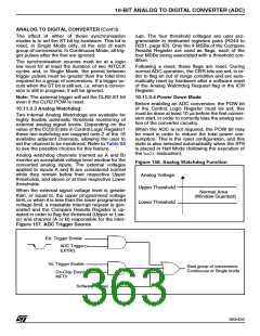
The ADC Interrupt Unit provides two maskable
channels (Analog Watchdog and End of Conver-
sion) with hardware fixed priority, and up to 7 pro-
grammable priority levels.
When the ST bit of Control Logic Register 2 is set,
either by software or by hardware (by an internal
or external synchronisation trigger signal), the an-
alog inputs are sequentially converted (from the
first selected channel up to channel 15) and the re-
sults are stored in the relevant pair of Data Regis-
ters.
Conversion Time
The maximum CKAD frequency allowable for the
analog part is 4 MHz. This is provided by a pro-
grammable prescaler that divides the ST9 system
clock (INTCLK) and a divider by 2. The user must
program the PR[2:0] bits in Control Logic Register
2 (CLR2, R253 - Page 63) to select the right pres-
caler dividing factor to obtain the correct clock fre-
quency for the analog part. Table 69 shows the
possible prescaling values and the related sam-
pling and conversion times. Generally, the formu-
las for the sampling and conversion times are:
In Single Mode (CONT = “0”), the ST bit is reset
by hardware following conversion of channel 15;
an End of Conversion (ECV) interrupt request is is-
sued and the ADC waits for a new start event.
In Continuous Mode (CONT = “1”), a continuous
conversion flow is initiated by the start event.
When conversion of channel 15 is complete,
conversion of channel 's' is initiated (where 's' is
specified by the setting of the SC[3:0] bits); this will
continue until the ST bit is reset by software. In all
cases, an ECV interrupt is issued each time
channel 15 conversion ends.
T
T
= (T
x 2) x (PR[2:0] x 8)
INTCLK
Sample
= (T
x 2) x (PR[2:0] x 28)
INTCLK
Conv
The user may need to increase the conversion
time if a resistor is added to the input pin, for in-
stance, as an overvoltage protection. In this case,
the ADC needs a longer sampling time to work
correctly.
When channel 'i' is converted ('s' <'i' <15), the re-
lated pair of Data Registers is reloaded with the
new conversion result and the previous value is
lost. The End of Conversion (ECV) interrupt serv-
ice routine can be used to save the current values
before a new conversion sequence (so as to cre-
ate signal sample tables in the Register File or in
Memory).
CAUTION: ADC INPUT PIN CONFIGURATION
The input Analog channel is selected by using the
I/O pin Alternate Function setting (PxC2, PxC1,
PxC0 = 1,1,1) as described in the I/O ports sec-
tion. The I/O configuration of the port connected to
the ADC converter is modified in order to prevent
the analog voltage present on the I/O pin from
causing high power dissipation across the input
buffer. Analog channels should be maintained in
Alternate Function configuration for this reason.
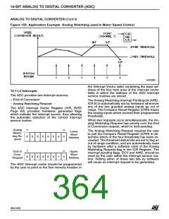
10.11.3.2 Triggering and Synchronisation
In both modes, conversion may be triggered by in-
ternal or external conditions; externally this may
be tied to EXTRG, as an Alternate Function input
on an I/O port pin, and internally, it may be tied to
INTRG, generated by a Multifunction Timer pe-
ripheral. Both external and internal events can be
separately masked by programming the EXTG/
INTG bits of the Control Logic Register (CLR). The
events are internally ORed, thus avoiding potential
hardware conflicts. However, the correct proce-
dure is to enable only one alternate synchronisa-
tion condition at any time.
10.11.3 Functional Description
10.11.3.1 Operating Modes
Two operating modes are available: Continuous
Mode and Single Mode. To enter one of these
modes it is necessary to program the CONT bit of
the Control Logic Register2 (CLR2, R253-
page63). The Continuous Mode is selected when
CONT is set, while Single Mode is selected when
CONT is reset.
362/426
9

 STMICROELECTRONICS [ ST ]